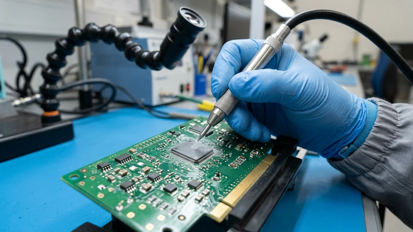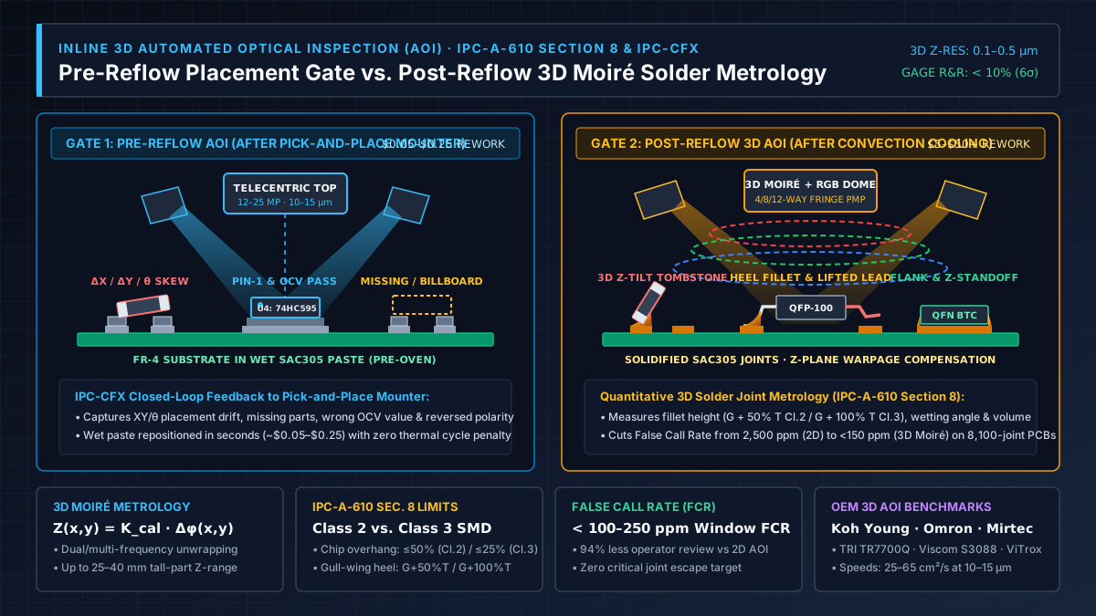
Running a high-density SMT assembly line without calibrated inline automated optical inspection (AOI) allows pick-and-place nozzle drift, reversed diode polarities, and reflow-induced tombstoning or lifted gull-wing leads to escape into in-circuit testing, causing expensive hot-air rework and board scrap. Modern 3D AOI systems combine multi-directional Phase-Measuring Profilometry (PMP / Digital Moiré fringe projection) with multi-angle RGB LED ring lighting and oblique side-view cameras to measure component placement offset, body coplanarity, and solder fillet volume at speeds of 25–65 cm²/s.
In a closed-loop surface-mount line, Pre-Reflow AOI sits immediately after the fine-pitch pick-and-place mounter and before the convection or vapor-phase reflow oven, catching missing parts, XY/theta skew, wrong OCV markings, and reversed polarity while the paste is still wet ($0.05 to $0.25 vacuum-tweezer correction with zero thermal stress). Post-Reflow 3D AOI sits after the oven cooling zone (board cooled below 40–50 °C to stabilize thermal warpage), using 4-way to 12-way multi-frequency Moiré fringes (0.1–0.5 µm Z-axis resolution across a 25–40 mm height range) and multi-angle RGB illumination to verify IPC-A-610 Section 8 solder meniscus wetting, heel fillet climb (G + 50% T for Class 2; G + 100% T for Class 3), and lead coplanarity while keeping window-level False Call Rates (FCR) below 100–250 ppm and Gage R&R below 10%.
For upstream thermal equipment sizing and zone architecture, see our pillar guide on reflow oven types and heated-tunnel sizing in the electronics manufacturing section.
| Inspection Gate / Metric | Pre-Reflow 3D AOI (Pre-Oven Gate) | Post-Reflow 3D AOI (Post-Oven Gate) | Upstream 3D SPI (Stencil Gate Baseline) |
|---|---|---|---|
| Inline SMT Position | After fine-pitch mounter, directly ahead of reflow oven entrance | After reflow cooling zone (board exit temp < 40–50 °C) |
Immediately after stencil printer, before pick-and-place |
| Physical State of Solder | Wet, un-reflowed SAC305 / SnBi tacky paste bricks | Solidified intermetallic solder fillet and meniscus | Unpopulated wet paste bricks (70–130% volume window) |
| Dominant Defects Captured | Missing parts, XY/theta offset, wrong OCV value, reversed polarity, flipped/billboarded chips, pre-shield cavity check | Solder bridges, tombstoning, lifted gull-wing leads, insufficient/excess fillet volume, de-wetting, QFN standoff tilt | Paste volume shortage/excess, pad bridging, slump, stencil aperture clog (< 0.66 area ratio) |
| Rework Cost & Thermal Stress | $0.05 to $0.25 per defect (5–10 s manual tweezer nudge; zero extra thermal cycle or pad lift) |
$5.00 to $50.00+ per defect (hot-air or iron desoldering, flux clean, second thermal excursion) |
$0.02 to $0.10 per board (ultrasonic solvent wipe and re-print before mounting parts) |
| Primary Optical Metrology | Telecentric top camera (10–15 µm) + 4/8-way 3D Moiré height & coplanarity + OCR/OCV |
Telecentric top camera (5.5–15 µm) + 4/8/12-way 3D Moiré + multi-angle RGB LEDs + 4 oblique side cameras (12–18 MP) |
Dual/quad-projection 3D phase-shift profilometry (0.1–0.3 µm Z-resolution) |
| IPC-2591 (IPC-CFX) Loop | Feeds real-time mean Delta X, Delta Y, and Delta theta drift back to mounter heads |
Correlates solidified fillet volume with 3D SPI paste volume and reflow thermal profile zones | Triggers automatic under-stencil wipe and X/Y/theta stencil alignment servo correction |
Where should automated optical inspection sit in an SMT assembly line?
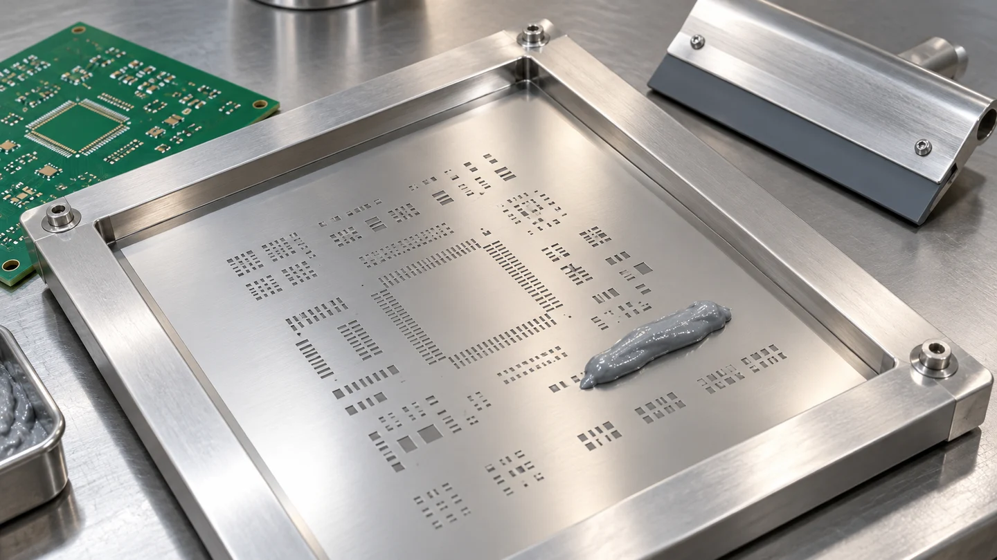
Deciding where to deploy automated optical inspection in an SMT assembly line depends on component density, RF shield topology, and the Rule of Tens rework cost escalation curve. Across high-volume electronics manufacturing, 70–75% of solder joint defects trace back to stencil printing variations (governed by solder paste powder size and the 0.66 area ratio), while the remaining 25–30% divide between pick-and-place machine kinematics and reflow soldering thermal profile defects.
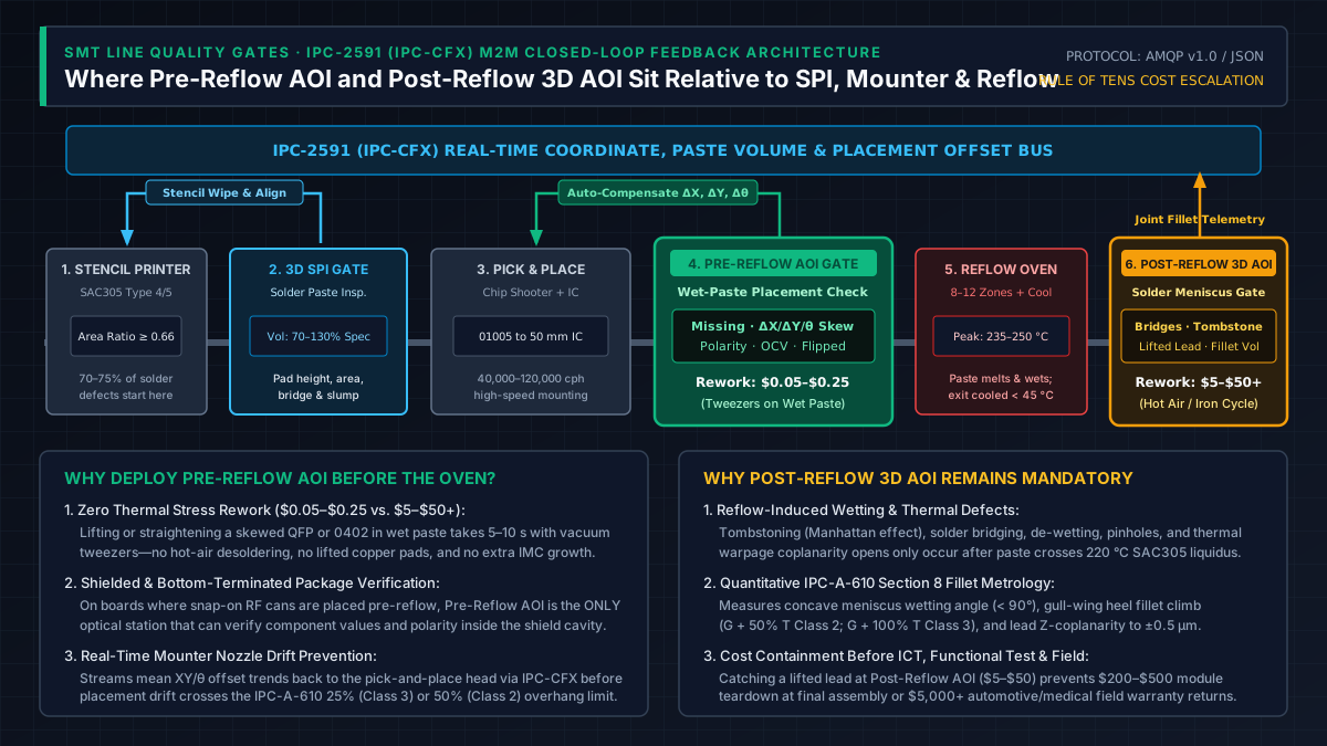
Gate 1: Pre-Reflow AOI (after pick-and-place, before the reflow oven)
Placed directly between the final flexible IC mounter and the entrance of the forced-convection or vapor-phase reflow oven, Pre-Reflow AOI inspects the populated board while the components sit in un-melted solder paste:
- Zero-thermal-shock rework economics (
$0.05to$0.25vs.$5.00to$50.00+): If a high-speed chip shooter drops a0201capacitor due to nozzle vacuum loss, places a diode backward, or skews a0.4 mm-pitch QFP by120 µm, an operator at the pre-reflow gate simply lifts or nudges the component with vacuum tweezers in5–10 seconds. Because the board has not entered the235–250 °CSAC305 reflow peak, rework causes zero copper land delamination, zero additional intermetallic compound (Cu6Sn5/Ag3Sn) thickening, and zero moisture-sensitivity degradation on neighboring ICs. - Un-occluded inspection inside RF shield cavities: On automotive radar, cellular baseband, and wireless IoT modules where stamped metal EMI/RF shield cans are machine-placed onto the board prior to reflow, Post-Reflow AOI cannot see through the solid metal lid. Pre-Reflow AOI positioned between the fine-pitch mounter and the shield-placement machine is the only optical gate capable of verifying component presence, polarity, and OCV part markings inside the shielded cavity.
- Closed-loop mounter drift compensation via IPC-CFX: Under IPC-2591 (Connected Factory Exchange), Pre-Reflow AOI measures the exact centroid (
X,Y,theta) of every placed package relative to the bare copper pad rather than the solder mask opening. When a feeder sprocket wears or a placement head nozzle warms up and drifts by25–40 µm, Pre-Reflow AOI transmits a JSON offset correction back to the mounter before any part crosses the IPC-A-610 overhang rejection boundary.
Gate 2: Post-Reflow 3D AOI (after the reflow oven cooling zone)
Even when Pre-Reflow AOI confirms 100% accurate placement into wet paste, thermal and capillary forces inside the reflow tunnel create defects that did not exist before the oven:
- Wetting and surface-tension defects created above liquidus (
217–220 °Cfor SAC305): As flux volatiles outgas and molten solder wets the metal terminations, unequal wetting torque between opposing pads pulls01005,0201, and0402passives upright into tombstones (the Manhattan effect) or rotates them on edge (billboarding). Simultaneously, paste slump or excessive pad volume coalesces into pin-to-pin solder bridges, while dynamic Z-axis warpage of the FR-4 laminate lifts gull-wing IC leads off their pads (open joints / coplanarity violations). - Board cooling prerequisite (
< 40–50 °C): Post-Reflow 3D AOI must sit downstream of the oven’s forced-air or water-chilled cooling modules so the PCB enters the optical stage below40–50 °C. Inspecting a board above60 °Cintroduces transient thermal creep in the FR-4 glass-epoxy matrix and shifts the refractive index of the air boundary layer beneath the telecentric lens. - Containing the Rule of Tens before ICT, coating, and final assembly: Reworking a post-reflow solder bridge or lifted QFP lead with a localized hot-air station or micro-iron costs
$5.00to$50.00+in technician labor and re-inspection. However, catching that defect at Post-Reflow 3D AOI prevents it from being sealed beneath conformal coating, passing into downstream through-hole wave soldering, or escaping to system-level functional test ($200to$500+teardown) and field warranty failure ($5,000+).
Rule of thumb: If your SMT line runs single-station AOI on low-mix consumer boards without pre-placed RF shields, place the 3D AOI post-reflow coupled with upstream 3D SPI; if you run high-mix boards, automotive/medical Class 3 assemblies, or RF-shielded modules with > 1,000 components per board, deploy both Pre-Reflow AOI and Post-Reflow 3D AOI.
Takeaway: Use 3D SPI and Pre-Reflow AOI to prevent defects while paste is wet (< $0.25 correction), and use Post-Reflow 3D AOI as the final quantitative IPC-A-610 Section 8 gate for solidified solder joints.
How do industrial 3D AOI equipment platforms compare?
Modern automated optical inspection hardware has transitioned from 2D top-down grayscale/color cameras to multi-projector 3D Phase-Measuring Profilometry (PMP / Digital Moiré) paired with high-resolution CoaXPress cameras and 4-way or 8-way oblique side-view optics. The table below benchmarks six industry-standard inline 3D AOI platforms used in high-volume SMT production.
| OEM & Benchmark Models | 3D Fringe Projection & Ring Lighting | Top & Side Camera Optics | Max 3D Height & Min Package | Inspection Speed & IPC-CFX Software Suite |
|---|---|---|---|---|
Koh Young Technology (Zenith 2, Zenith Alpha, Zenith UHS) |
True 3D Multi-Frequency Moiré phase-shift profilometry (8-way projection on Zenith 2 / UHS; 5-way on Zenith Alpha) + multi-color LED dome |
8 MP, 12 MP, or 25 MP telecentric top camera (15 µm or 20 µm pixel size) + optional 4-way 12 MP side-view cameras |
Up to 25 mm programmable height; inspects down to 01005 Imperial (0402M) and 0201M with local pad warp compensation | 29.1–49.9 cm²/s (Zenith 2), 23.1–55.3 cm²/s (Zenith Alpha), ultra-high-speed on UHS; KSMART, KAP AI auto-programming & KPO closed-loop optimizer |
Omron Automation (VT-S1080, VT-S730, VT-S530) |
4-directional Micro Phase Shift (MPS / Multi-Direction Moiré) 3D projectors + proprietary MDMC Color Highlight™ multi-angle RGB LED rings |
25 MP top telecentric camera + 4 x 5 MP oblique side cameras on VT-S1080 (4 MP / 12 MP options on VT-S730 / VT-S530) |
Up to 25 mm component height; extracts true 3D fillet volume plus IPC-A-610 wetting angle via MDMC specular color gradient | High-speed hybrid 2D Color Highlight + 3D phase-shift capture; AI threshold self-tuning & Q-up Navi M2M root-cause traceability |
Mirtec (MV-6 OMNI Inline, MV-3 OMNI Benchtop) |
OMNI-VISION® 12-projection Digital Blue Light Multi-Frequency Moiré + 8-phase coaxial color LED lighting system |
15 MP or 25 MP CoaXPress top camera (7.7 µm, 10 µm, or 15 µm telecentric lens) + Side-Viewer® 4 x 18 MP angled cameras |
0–25 mm shadow-free 3D height range; closed-loop AC linear/servo stage with 1 µm XY positioning resolution |
High-frame-rate CoaXPress Turbo Speed capture; Intelli-PRO AI auto-programming & TRMS (Total Remote Management System) |
Test Research, Inc. — TRI (TR7700Q SII, TR7700QE) |
Quad (4-way) Adaptive Digital Fringe Pattern Projectors with Depth from Focus (DFF) + multi-phase true color LED lighting |
12 MP CoaXPress top camera (5.5 µm, 9.8 µm, 10 µm, 12 µm, or 15 µm factory optical resolution) + 4 angled side cameras |
Up to 40 mm 3D height range on TR7700QE (0.6–5.0 mm PCB thickness capacity, eliminating tall-connector blind spots) |
Up to 57 cm²/s at 15 µm (~37 cm²/s at 12 µm, ~25 cm²/s at 10 µm); YMS 4.0 (Yield Management System) & IPC-CFX M2M |
Viscom AG (S3088 ultra chrome, S3088 ultra gold) |
XM / XMplus 3D structured-light fringe projection module (up to 3.6 Gigapixels/s throughput) + multi-angle LED illumination |
9-camera array (1 orthogonal top camera at 10 µm/pixel + 8 angled-view cameras totaling up to 121 MP combined) |
Up to 30 mm Z-range with 0.5 µm Z-height resolution; inspects down to 03015M (008004 Imperial) micro-passives | Up to 65 cm²/s inspection speed with FastFlow board handling (2.0–2.5 s exchange); vVision, vVerify & Quality Uplink |
ViTrox Technologies (V510i Optimus 3D AOI) |
4-way high-speed Phase Shift Profilometry (PSP) structured-light projectors + multi-angle color ring illumination |
12 MP CoaXPress top camera (15 µm telecentric lens default, 60 x 45 mm FOV; optional 8 µm or 13 µm lenses) + 4 side cameras |
Full 3D volumetric pad, body, and solder fillet height profiling with dynamic real-time PCB warpage compensation | Up to 60–64 cm²/s at 15 µm resolution; V-One Industry 4.0 platform with A.I. VVTS automated false-call verification |
Three optical engineering specifications govern machine selection when comparing vendor datasheets:
- Pixel resolution (
µm/pixel) vs. field of view (FOV) and line takt time: Optical resolution and inspection speed trade off quadratically because halving pixel size from15 µmto7.5 µmdivides the single-frame FOV area by four. For standard0201 Imperial (0603M)and0.4 mm-pitch QFP assembly, a 12–25 MP camera with a 12–15 µm telecentric lens delivers45–65 cm²/sthroughput while placing16 x 8pixels across a0.25 x 0.125 mm01005termination. Ultra-fine008004 Imperial (0201M)or03015Mdie-level assembly requires a 5.5–10 µm optical lens (such as on TRITR7700Q SII, MirtecMV-6 OMNI, or ViscomS3088 ultra chrome). - Projector count (
4-wayvs.8-wayvs.12-way) and tall-part clearance: When a0201chip resistor sits0.5 mmaway from a20 mm-tall aluminum electrolytic capacitor or automotive header, a single or dual projector casts an optical shadow across the chip. Systems using 4-way to 12-way radial Moiré projectors (Koh Young8-wayZenith 2, Mirtec12-wayMV-6 OMNI) reconstruct the 3D height profile from the un-occluded opposing projectors, while platforms like TRITR7700QEextend Depth-from-Focus Z-range up to 40 mm. - Oblique side-view cameras (
4-wayvs.8-wayat45°–60°): An orthogonal90°top-down telecentric lens cannot see underneath the tucked knee of a PLCC J-lead, the vertical side cavity of a wettable-flank QFN, or a tall QFP heel fillet shadowed by the IC body overhang. Specifying4to8angled side cameras (5 MPto18 MPeach) provides direct line-of-sight metrology into vertical side meniscuses.
Rule of thumb: If your board mix includes 01005 Imperial (0402M) passives or 0.3–0.4 mm fine-pitch QFPs/QFNs alongside tall (> 15 mm) connectors, specify a 3D AOI with <= 10–12 µm optical pixel resolution, at least 4- to 8-way fringe projection, and 4 angled side-view cameras.
Takeaway: Benchmark 3D AOI platforms at the exact optical resolution (10 µm vs. 15 µm) required by your smallest SMD pad—never compare raw cm²/s datasheet speeds recorded at different pixel sizes.
How do 3D Moiré phase-shift profilometry and multi-angle RGB lighting work?
To understand why legacy 2D AOI systems struggle with 2,500–20,000 ppm false alarm rates while modern 3D AOI platforms hold window False Call Rates below 100–250 ppm, process engineers must examine how light interacts with a solidified SAC305 solder meniscus.
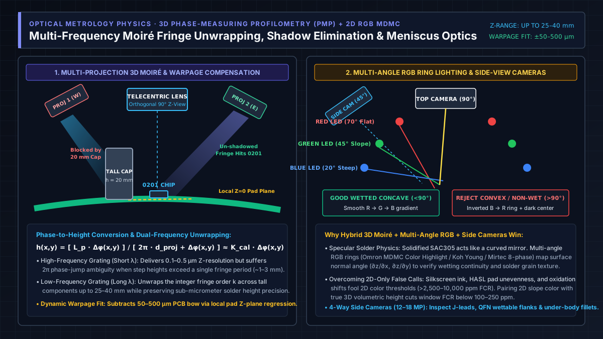
2D Multi-Angle RGB LED ring lighting (MDMC / Color Highlight)
A solidified solder joint is not a diffuse Lambertian surface like paper or matte plastic; it is a curved metallic mirror. Under Multi-Direction Multi-Color (MDMC) illumination (pioneered by Omron’s Color Highlight™ and integrated across modern hybrid AOI domes), concentric LED rings emit Red light at a steep near-vertical angle (~65°–80°), Green light at a medium oblique angle (~40°–50°), and Blue light at a low grazing angle (~15°–25°):
- Wetted concave solder fillet (
< 90°wetting contact angle): Because a properly wetted solder fillet curves smoothly from horizontal at the copper land toe to steep at the component lead knee, the flat pad reflects Red light upward into the telecentric top camera, the45°concave belly reflects Green light, and the steep heel climb reflects Blue light. The camera sees a predictableRed -> Green -> Bluecolor-phase sequence that maps surface slope (dz/dx,dz/dy). - Un-wetted convex / cold / excess solder joint (
> 90°contact angle): A convex solder ball or non-wetted pad bulges outward, inverting the specular reflection sequence (Blue -> Green -> Red) or leaving a dark non-reflective center. - Why 2D color slope alone triggers false calls: Lead-free SAC305 (
Sn96.5/Ag3.0/Cu0.5, detailed in our solder paste alloy and powder size guide) cools with a rougher, grainier crystalline surface than eutecticSn63/Pb37, scattering incident LED rays. Furthermore, 2D RGB intensity cannot measure absolute Z-height in micrometers: a white silkscreen line next to a0201resistor, thickness variations on hot-air solder leveled (HASL) pads, or dark-body vs. light-body vendor substitutions fool 2D grayscale and color thresholds.
3D Phase-Measuring Profilometry (PMP) and multi-frequency Moiré unwrapping
True 3D AOI eliminates 2D reflectivity ambiguity by projecting sinusoidal structured-light fringe patterns (I_n(x, y)) from 4, 8, or 12 angled projectors onto the PCB and capturing N phase-shifted images (typically 4-step to 12-step phase shifting) on the orthogonal telecentric camera.
For a 4-step phase-shift sequence with phase steps of 0, pi/2, pi, and 3*pi/2 radians, the wrapped phase phi(x, y) at every pixel (x, y) is computed directly from the four intensity frames I_1, I_2, I_3, I_4:
phi(x, y) = arctan2( I_4(x, y) - I_2(x, y), I_1(x, y) - I_3(x, y) )Because I_4 - I_2 and I_1 - I_3 cancel out background ambient light I_bg(x, y) and surface reflectivity contrast R(x, y), the extracted phase shift Delta_phi(x, y) between the component/solder surface and the local PCB reference plane is mathematically independent of whether the surface is shiny SAC305 solder, matte black epoxy, or bright white silkscreen. The triangulation geometry then converts phase shift Delta_phi(x, y) into physical height h(x, y):
h(x, y) = ( L_p * Delta_phi(x, y) ) / ( 2 * pi * d_proj + Delta_phi(x, y) ) ~= K_cal * Delta_phi(x, y)where L_p is the projector-to-reference-plane working distance, d_proj is the baseline offset between projector and camera optical axes, and K_cal = P_eff / (2 * pi) is the calibrated effective fringe pitch constant (in µm/rad).
To resolve both sub-micrometer solder fillets and 25–40 mm tall connectors simultaneously, industrial 3D AOI uses dual- or multi-frequency phase unwrapping:
- High-frequency (short-wavelength) fringe grating (
P_short ~ 0.8–2.0 mm): Provides fine vertical sensitivity (0.1–0.5 µm Z-resolution), ideal for measuring a35 µmlifted QFP lead or01005chip tilt. However, whenever a component step exceeds one fringe wavelength (Delta_phi > 2*pi), the arctangent function wraps around (2*piambiguity). - Low-frequency (long-wavelength) fringe grating (
P_long ~ 15–40 mm): Projects a wide fringe period that spans the entire 25–40 mm height envelope without wrapping, determining the exact integer fringe orderkso the high-frequency phase is unwrapped (Phi_unwrapped = phi_short + 2 * pi * k). - Dynamic local Z-plane warpage compensation: During reflow, thermal expansion mismatches bow and twist FR-4 boards by 50–500+ µm across the panel. Rather than referencing a fixed machine stage height, 3D AOI samples copper or solder-mask fiducial lands within
1–3 mmaround each component, fits a local 3D plane (Z_local(x, y) = a*x + b*y + c), and computes component standoff, lead coplanarity, and solder fillet volume (V = sum(h_i * A_pixel)) relative to that local plane.
Worked example: 3D Moiré height calculation and Gage R&R check on a lifted QFP lead
Suppose a Post-Reflow 3D AOI with a 12 µm/pixel telecentric lens (A_pixel = 12 µm * 12 µm = 144 µm²) inspects a 0.5 mm-pitch LQFP-100 gull-wing IC.
- High-frequency effective fringe pitch
P_eff = 1,256.6 µm(1.2566 mm), yielding a phase-to-height calibration constant:
K_cal = P_eff / (2 * pi) = 1,256.6 µm / 6.2832 rad = 200.0 µm/rad- Around Pin 18, the local PCB reference plane regression across adjacent bare solder-mask pads defines
Z_local = 0.0 µm. - On neighboring normal leads (Pins 17 and 19), the top of the gull-wing foot measures a phase shift
Delta_phi_normal = 0.900 rad:
Z_normal = 200.0 µm/rad * 0.900 rad = 180.0 µm (150 µm lead thickness T + 30 µm solder paste fillet G)- On Pin 18, the gull-wing toe has sprung upward during reflow cooling (a lifted lead open joint), producing a measured phase shift
Delta_phi_pin18 = 1.240 radwhile the underlying pad showsDelta_phi_pad18 = 0.110 rad(Z_pad18 = 22.0 µmof un-wetted solidified solder):
Z_pin18     = 200.0 µm/rad * 1.240 rad = 248.0 µm
Delta_Z_lift = Z_pin18 - Z_normal       = 248.0 µm - 180.0 µm = +68.0 µm lead coplanarity lift
Because +68.0 µm exceeds the programmed 40 µm coplanarity lift ceiling and the side-view camera records zero heel meniscus climb bridging the 22.0 µm pad solder to the lifted foot, the 3D AOI flags Pin 18 as a true open-joint defect.
To qualify this 3D height measurement under AIAG Measurement Systems Analysis (MSA) standards across a ±50 µm (100 µm total tolerance window T_tol) coplanarity specification, a 10-part, 3-run, 3-trial Gage R&R study records a combined equipment repeatability and reproducibility standard deviation sigma_GRR = 1.15 µm:
%GR&R = (6 * sigma_GRR / T_tol) * 100% = (6 * 1.15 µm / 100.0 µm) * 100% = 6.90%Because 6.90% is strictly below the 10% Gage R&R acceptance threshold (< 10% acceptable; 10–30% marginal; > 30% unacceptable), the 3D Moiré sensor is statistically capable of enforcing the 40 µm lift gate without generating false calls.
Rule of thumb: Never accept a 3D AOI program into production based solely on visual defect capture; require a quantitative Gage R&R < 10% on 3D height and volume across golden boards and verify that local Z-plane warpage compensation is enabled on every fine-pitch IC.
Takeaway: Hybrid 3D AOI combines multi-frequency Moiré profilometry (Z = K_cal * Delta_phi) for absolute height and volume with multi-angle RGB rings for wetting-angle verification.
SMD vs SMT in AOI programming: How does IPC-A-610 Section 8 judge each package family?
When building inspection libraries, process engineers frequently encounter confusion around SMD vs SMT terminology:
- SMT (Surface Mount Technology) is the complete board-level manufacturing methodology—covering stencil design, solder paste printing, high-speed pick-and-place mounting, convection or vapor-phase reflow soldering, and inline 3D SPI/AOI inspection.
- SMD (Surface Mount Device) is the individual physical component package engineered to solder onto planar surface copper lands without plated through-holes (as opposed to through-hole technology components governed by IPC-A-610 Section 7; see our wave vs reflow soldering process guide).
In automated optical inspection, that distinction is operational: an SMT line runs one unified board conveyor, but the AOI vision engine must apply a completely different 2D/3D mathematical inspection algorithm and IPC-A-610 Section 8 (Surface Mount Assemblies) acceptance threshold to each SMD package family.
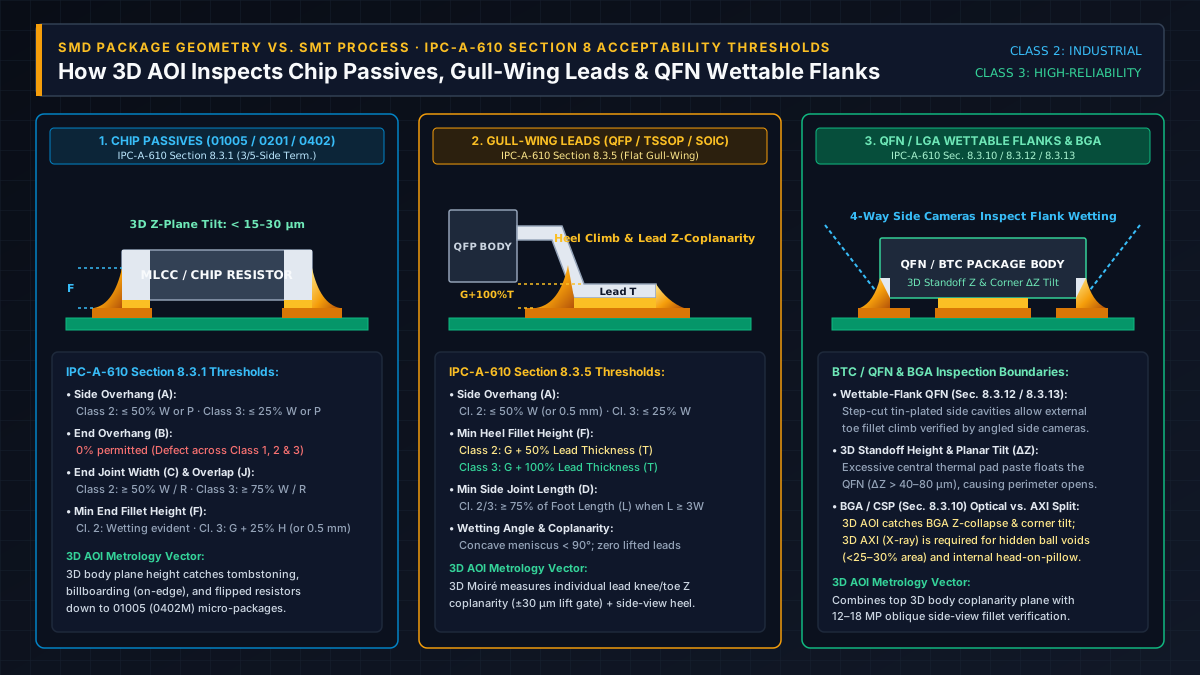
IPC-A-610 Section 8 Class 2 vs. Class 3 SMD inspection matrix
| SMD Package Family & IPC-A-610 Section | Max Side Overhang (A) & End Overhang (B) |
Min End Joint Width (C) / Side Length (D) |
Min Solder Fillet Height (F) & Wetting |
3D AOI Metrology Vector & Optical Gate |
|---|---|---|---|---|
Rectangular / Square Chip Passives (01005, 0201, 0402, 0603, 0805 MLCCs & Resistors) — Section 8.3.1 |
Side (A): <= 50% of termination width W or land P (Class 2); <= 25% W or P (Class 3)End ( B): 0% permitted (Defect for Class 1/2/3) |
End Width (C): >= 50% W or P (Class 2); >= 75% W or P (Class 3)End Overlap ( J): >= 50% R (Cl. 2); >= 75% R (Cl. 3) |
Class 2: Properly wetted fillet evident Class 3: Solder thickness G + 25% of termination height H or 0.5 mm (whichever is less) |
3D Z-plane body tilt (> 15–30 µm delta Z) catches early tombstoning and billboarding; 3D fillet volume + RGB slope verifies end wetting; 2D dark/light contrast catches flipped resistors |
Flat Gull-Wing Leaded ICs (SOIC, TSSOP, QFP, LQFP) — Section 8.3.5 |
Side (A): <= 50% of lead width W or 0.5 mm (Class 2); <= 25% W or 0.5 mm (Class 3)Toe ( B): May not violate min electrical clearance |
End Width (C): >= 75% W (Class 2/3)Side Length ( D): >= 75% of foot length L when L >= 3W (>= 100% L when L < 3W Cl. 3) |
Min Heel Height (F):Class 2: G + 50% lead thickness TClass 3: G + 100% lead thickness T (reaches top of heel knee) |
3D Moiré measures every lead knee/toe Z-height (>= 30–50 µm coplanarity lift gate) and pin-to-pin bridging; 4-way side cameras inspect heel fillet climb F |
Round or Flattened J-Lead Packages (PLCC, SOJ) — Section 8.3.6 |
Side (A): <= 50% of lead width W (Class 2); <= 25% W (Class 3) |
End Width (C): >= 75% W (Class 2/3)Side Length ( D): >= 150% W (Class 2/3) |
Min Heel Height (F):Class 2: G + 50% lead thickness TClass 3: G + 100% lead thickness T |
Requires 4-direction angled side cameras (45°–60°) because the J-bend curls underneath the IC package perimeter out of top-down view |
Bottom-Terminated Components — BTC (QFN, DFN, SON, LGA) — Section 8.3.12 / 8.3.13 |
Side (A) & Toe (B): <= 50% W (Class 2); <= 25% W (Class 3); thermal pad voiding (< 25–30%) requires 3D AXI |
End Joint Width (C): >= 50% W (Class 2); >= 75% W (Class 3) on exposed perimeter lands |
Flat bottom only: Wetting evident at toe Wettable Flank (Sec. 8.3.13): Side/toe fillet climb evident up step-cut cavity |
3D AOI measures package body standoff height (Z) and corner-to-corner planar tilt (Delta Z > 40–80 µm) caused by excess central thermal pad paste floating the QFN; side cameras verify wettable-flank fillets |
Area Array Packages (BGA, CSP, PoP) — Section 8.3.10 |
Ball-to-land alignment within ball pitch clearance; hidden ball voids and head-on-pillow require 3D AXI (X-ray) | Uniform ball collapse and full wetting to package and PCB lands without bridging | Uniform standoff height G across package array without corner lift or center sag |
Pre-reflow AOI checks XY/theta & OCV; Post-reflow 3D AOI measures BGA body Z-collapse height and dynamic warpage tilt across all 4 corners to flag bridged or un-collapsed rows |
Why QFN and BGA packages require both 3D standoff metrology and side-camera or AXI boundaries
A frequent mistake in SMT inspection planning is assuming that top-down optical cameras cannot provide any diagnostic data on bottom-terminated QFN or BGA packages—or conversely, assuming that AOI replaces X-ray (3D AXI) for hidden thermal pads:
- Catching QFN “floating” via 3D body Z-standoff and corner tilt: On a QFN package (
IPC-A-610 Section 8.3.12), if the stencil aperture on the central ground/thermal pad deposits excess solder paste (instead of being window-paned into50–80%area coverage; see matching stencil apertures and paste), the molten central solder pillow floats the QFN upward during reflow. Even if the perimeter lands lack wettable flanks, a 3D Moiré AOI immediately detects that the QFN package body sits 50–120 µm higher than nominalZ_standoffor exhibits > 40–80 µm corner-to-corner tilt (Delta Z), flagging perimeter open joints that a 2D camera never sees. - Wettable-flank QFN inspection (
IPC-A-610 Section 8.3.13): Automotive Class 3 assemblers specify QFN packages with step-cut tin-plated wettable flanks so that molten solder climbs up the exterior side wall of each perimeter termination. By combining4-wayoblique side cameras (12–18 MPon Koh Young, Mirtec, TRI, Viscom, and ViTrox platforms) with 3D volumetric toe fillet profiling, 3D AOI verifies external QFN wetting at inline SMT speeds without slowing the line for 100% X-ray inspection. - Where 3D AXI (Automated X-Ray Inspection) remains mandatory: Optical photons cannot penetrate silicon dies or FR-4 epoxy. Therefore, verifying internal BGA ball voiding (
< 25%or< 30%area per IPC-A-610 Section 8.3.10), hidden BGA head-on-pillow microstructure, or QFN central thermal-pad void percentages requires inline or offline 3D Computed Tomography (CT) AXI.
Rule of thumb: Program 3D AOI to enforce a ±40–60 µm Z-standoff and planar tilt window on every QFN, LGA, and BGA package body on the board—it catches stencil thermal-pad over-printing and package warpage opens at zero extra cycle time.
Takeaway: Map every CAD footprint in your AOI library to its exact IPC-A-610 Section 8 package class (8.3.1 chips, 8.3.5 gull-wing, 8.3.6 J-lead, 8.3.12/8.3.13 QFN/BTC) rather than sharing generic pass/fail thresholds across SMD families.
How do you calculate False Call Rate (FCR), Escape Rate, and IPC-CFX closed-loop ROI?
In production SMT operations, an automated optical inspection program is governed by two competing statistical metrics: Escape Rate (true IPC-A-610 defects that pass through the machine undetected) and False Call Rate (FCR) (conforming IPC-A-610 joints that the machine erroneously flags as defects, forcing human review).
Window-Level FCR (ppm) = ( N_false_calls / N_total_inspected_windows ) * 10^6
Board-Level FCR (%)    = ( N_boards_with_>=1_false_call / N_total_boards_inspected ) * 100%
Escape Rate (ppm)      = ( N_escaped_true_defects / N_total_inspected_joints ) * 10^6
Why is lowering window-level FCR below 100–250 ppm critical to preventing defect escapes? When a poorly tuned AOI bombards the review station operator with 15–30 false alarms on every single board, human confirmation bias sets in (operator alarm fatigue): the operator begins tapping the “Pass / Clear All” hotkey at high speed and accidentally clears the rare true lifted lead or tombstone hidden among the false alarms.
Worked example: 2D AOI vs. 3D Moiré AOI false-call math on an 8,100-window PCBA
Consider an automotive infotainment SMT line running at a 30 s cycle time (120 boards/hour, or 960 boards per 8-hour shift). Each board carries N_comp = 1,800 SMD components with an average of 4.5 inspection windows per component (two termination fillets + two side/end overhang checks + one body/polarity window on passives, plus individual pin windows on QFPs), totaling:
N_windows_per_board = 1,800 components * 4.5 windows/component = 8,100 inspection windows/board
N_windows_per_shift = 8,100 windows/board * 960 boards/shift   = 7,776,000 windows/shift
Scenario A — Legacy 2D RGB AOI running at FCR_2D = 2,500 ppm (0.25% per window):
- False calls generated per board:
False_Calls_Board_2D = 8,100 * (2,500 / 1,000,000) = 20.25 false calls/board- Using the Poisson / binomial probability approximation
P(>=1 false call) = 1 - exp(-20.25) ~= 100%, virtually 100% of good boards are diverted to the manual review station. - At
3.0 secondsof operator visual verification per flagged window, each board consumes20.25 * 3.0 s = 60.75 sof review labor—exceeding the30 sline takt time and requiring two full-time review operators per line (19,440 false calls/shift = 16.2 operator hours/shift).
Scenario B — 3D Multi-Frequency Moiré AOI tuned to FCR_3D = 150 ppm (0.015% per window):
- False calls generated per board:
False_Calls_Board_3D = 8,100 * (150 / 1,000,000) = 1.215 false calls/board- Total false calls across the
960-boardshift drop from19,440to1,166(a 94.0% reduction in false alarms). - Operator verification time drops to
1.215 * 3.0 s = 3.65 s/board(0.97 hoursper8-hourshift), allowing a single operator or centralized AI verification hub (such as Koh YoungKSMART, ViscomvVerify, or ViTroxA.I. VVTS) to manage four to six SMT lines simultaneously while holding critical joint Escape Rate at 0 ppm.
Root-cause isolation across 3D SPI, Mounter, and 3D AOI via IPC-CFX
Connecting 3D SPI, pick-and-place mounters, Pre-Reflow AOI, and Post-Reflow 3D AOI over IPC-2591 (IPC-CFX) transforms AOI from a passive end-of-line sorting gate into an active process stabilizer:
| Post-Reflow 3D AOI Defect Signature | Upstream 3D SPI & Pre-Reflow AOI Telemetry Match | Isolated Root Cause & Automated Corrective Action |
|---|---|---|
0201 / 0402 Tombstoning (Delta Z > 150 µm) |
Case 1: 3D SPI shows Pad A paste volume = 62% and Pad B = 118%Case 2: 3D SPI paste volumes equal ( 98% / 101%), Pre-Reflow AOI shows 85 µm X-offsetCase 3: Both SPI and Pre-Reflow AOI nominal |
Case 1: Partial stencil aperture clog; trigger under-stencil wet/vacuum wipe (check paste storage and viscosity). Case 2: Mounter nozzle offset; IPC-CFX sends -85 µm X-compensation to placement head.Case 3: Excessive reflow preheat/reflow thermal gradient or nitrogen wetting imbalance (audit reflow profile). |
| Fine-Pitch QFP Pin-to-Pin Bridging | Case 1: 3D SPI shows paste height > 135% and slumped edge bridging pre-placeCase 2: SPI normal, Pre-Reflow AOI shows excessive Z-overdrive placement pressure smearing paste |
Case 1: Stencil separation speed or squeegee pressure out of spec; adjust printer recipe. Case 2: Mounter Z-axis placement height set too deep into wet paste; raise placement Z-stop by 30–50 µm. |
Gull-Wing Lifted Lead (Coplanarity > 40 µm) |
Case 1: Pre-Reflow AOI 3D lead measurement already shows bent/lifted pin prior to oven Case 2: Pre-Reflow AOI shows flat lead sitting in paste, lift appears only Post-Reflow |
Case 1: Incoming SMD tray/tape handling damage or bent lead at pick nozzle. Case 2: Dynamic PCB warpage during reflow peak/cooling; adjust center support pins or reflow cooling slope. |
Rule of thumb: Do not allow operators to widen IPC-A-610 Section 8 height or overhang limits just to silence false calls on the shop floor; instead, lock IPC thresholds at the engineering level, verify local Z-plane warpage reference pads, and tune 3D ROI (Region of Interest) pad registration against CAD Gerber data.
Takeaway: Track window-level FCR in ppm alongside Gage R&R (< 10%) and link 3D SPI, Pre-Reflow AOI, and Post-Reflow 3D AOI via IPC-CFX so stencil and mounter drift are corrected before they create solder rework.
Related reading
- Reflow oven types and how to choose one for PCB assembly — Forced-convection, infrared, and vapor-phase reflow architectures plus heated-tunnel length sizing.
- Reflow soldering process stages and temperature profile — Preheat, soak, reflow, and cooling thermal limits and profile-induced defect maps.
- Solder paste types guide: alloy, flux, and powder size — How Type 3, 4, 5, and 6 solder powders and the
0.66area ratio govern upstream 3D SPI yield. - Solder paste alloy and powder size selection — Matching SAC305 and low-temperature pastes to fine-pitch
01005and0.4 mmQFP stencil apertures. - Wave vs reflow soldering: choose a process for each part — Assigning SMD and through-hole packages across reflow, mass wave, selective, and hand soldering.
- Wave soldering machine preheat and dual-wave contact — Downstream through-hole spray fluxing, preheat slopes, dual-wave dwell, and IPC-A-610 Section 7 barrel fill.
- Electronics manufacturing guides — Browse all PCBA assembly, soldering, and optical inspection guides on the EMT WorldWide blog.