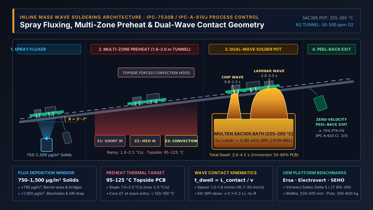
Running a printed circuit board assembly across a molten solder wave with wrong preheat slopes or unbalanced nozzle dwell causes incomplete vertical barrel fill, pin-to-pin bridging, blowholes, and costly board rework. A production wave soldering machine synchronizes four inline stages—ultrasonic spray fluxing, multi-zone infrared and forced-convection preheating, dual-wave solder pot contact, and inclined peel-back exit—so that plated through-hole (PTH) barrels fill to IPC-A-610 acceptance limits without thermally shocking components or leaching barrel-knee copper.
In a standard lead-free SAC305 wave soldering process, an ultrasonic or reciprocating spray fluxer deposits 750–1,500 µg/in² (120–240 µg/cm²) of dry active flux solids onto the board underside. A modular 1.8–3.0 m preheat tunnel then warms the assembly at 1.0–2.5 °C/s to a topside PCB temperature of 95–125 °C (90–110 °C for alcohol-based no-clean fluxes; 110–125 °C for VOC-free water-based fluxes). The board travels up a 5°–7° inclined finger or pallet conveyor at 1.0–1.8 m/min (16.7–30.0 mm/s) across a 255–265 °C solder pot, spending 0.8–1.5 s in the turbulent chip wave and 2.0–3.5 s in the laminar smooth wave (3.0–4.5 s total dwell) at 50–80% board thickness immersion.
For part-level process assignment between surface-mount reflow, mass wave, selective dip/nozzle, and hand soldering, start with our pillar comparison on wave soldering vs reflow in the electronics manufacturing section.
| Process Stage / Parameter | Standard Lead-Free SAC305 Window | Eutectic Sn63/Pb37 Baseline | Governing Mechanism & Dominant Risk |
|---|---|---|---|
| Spray Flux Solids Deposition | 750–1,500 µg/in² (120–240 µg/cm²) | 600–1,200 µg/in² | < 750 µg/in² starves barrel wetting and causes bridges; > 1,500 µg/in² traps solvent and drops SIR |
| Topside Preheat Exit Temp | 95–125 °C (up to 130–140 °C heavy Cu) | 85–105 °C | Must evaporate carrier (especially water at 100 °C) and activate rosin/resin before wave entry |
| Preheat Thermal Ramp Rate | 1.0–2.5 °C/s (<= 3.0 °C/s hard ceiling) |
1.0–2.5 °C/s | Exceeding 2.5–3.0 °C/s fractures MLCC chip capacitors and delaminates FR-4 glass-epoxy |
Core Thermal Shock (Delta T) |
<= 130–150 °C (solderside to pot) | <= 130 °C | Pre-bath convection platen prevents temperature drop between final heater and Wave 1 |
| Solder Pot Temperature | 255–265 °C (liquidus 217–220 °C) | 245–255 °C (liquidus 183 °C) | Provides 35–45 °C superheat above liquidus; > 265 °C accelerates PTH knee copper dissolution |
| Wave 1 (Turbulent Chip) Dwell | 0.8–1.5 s | 0.5–1.2 s | High-velocity vertical jets scrub flux vapor pockets and wet tight bottom-side SMD pads |
| Wave 2 (Laminar Main) Dwell | 2.0–3.5 s | 1.5–2.5 s | Broad bidirectional/Lambda wave drives vertical capillary fill and zero-velocity peel-back |
| Combined Total Wave Dwell | 3.0–4.5 s (max 5.0 s heavy multilayer) | 2.0–3.5 s | Controlled by t_dwell = L_contact / v_conveyor; > 5.0 s leaches barrel copper |
| Conveyor Speed & Angle | 1.0–1.8 m/min at 5°–7° tilt | 1.2–2.0 m/min at 5°–7° | Sets drainage velocity at wave exit; shallow angles (< 4.5°) leave pin-to-pin bridges |
| Bath Copper Impurity Limit | 0.75–0.85 wt% Cu (start 0.50 wt%) | Max 0.30 wt% Cu | > 0.85 wt% Cu precipitates Cu6Sn5 needles, raising liquidus by 6–10 °C |
How do industrial wave soldering equipment platforms compare?
Selecting wave soldering equipment requires matching conveyor working width, active preheat length, nozzle programmability, and nitrogen inerting architecture to board thermal mass and line takt time. While forced-convection reflow ovens from vendors such as Heller Industries handle upstream surface-mount paste reflow (covered in where a wave soldering machine fits next to a reflow oven), mass wave soldering relies on dedicated molten-bath platforms from Kurtz Ersa, Electrovert (ITW EAE), Vitronics Soltec (ITW EAE), SEHO Systems, JT Automation, and Folungwin.
| OEM & Benchmark Models | Max Working Width | Active Preheat Architecture | Solder Pot, Nozzle Geometry & N2 Inerting |
|---|---|---|---|
Kurtz Ersa (POWERFLOW ULTRA, POWERFLOW N2 XL, POWERFLOW PRO) |
PRO: 330 / 400 / 458 mm; N2 XL: up to 508–520 mm; ULTRA XXL: wide-board |
Modular 1,800–3,000 mm tunnel (3–4 zones on PRO/N2 XL; up to 3,000 mm on ULTRA) combining short-wave IR, medium-wave IR cassettes, and forced convection with ERSASOFT 5 compensation |
Enamelled stainless lead-free exchangeable pot (525–630 kg on PRO, ~820 kg on N2 XL, max 300 °C); dual-wave axis drives (5 mm/s) with VarioWave; full closed N2 tunnel (16–20 m³/h typical on N2 XL) |
Electrovert / ITW EAE (Electra, VectraElite) |
VectraElite: 457 mm (508 mm opt.); Electra: 508 mm (610 mm opt.) |
Modular front-accessible zones up to 2,400 mm (8 ft) bottom-side and 1,800 mm (6 ft) top-side combining IsoThermal forced convection (ICP heat-on-intake platens) and Fast Response IR |
Cast lead-free pot with titanium internals; Lambda, OptiWave, DwellMax 4.0, DwellFlex 4.0 (adjustable contact length), UltraFill 4.0, Deep Wave (up to 20 mm height for thick pallets), EcoWave exit wing (50–75% dross cut), and ExactaWave closed-loop height sensor |
Vitronics Soltec / ITW EAE (Delta 5 Mass Wave vs. ZEVAm Selective) |
Delta 5: up to 457–508 mm standard mass conveyor |
Delta 5: 3-zone PID modular preheat up to 1,800 mm (6 ft) pairing bottom/top forced air convection, Calrod, and quartz/IR lamps immediately ahead of the wave |
Titanium lead-free dual-wave pot (turbulent Chip Wave + laminar Lambda/SmartWave), mechanical dross separation, automatic 2-bar feeder, and optional NitroWave hood (whereas ZEVAm uses selective electromagnetic mini-pots for < 1 mm pitch clearances) |
SEHO Systems (PowerWave N2, GoWave 1030, MWS 2340) |
GoWave 1030: 300–340 mm; PowerWave N2 & MWS 2340: 400–500 mm |
GoWave: compact 700 mm IR (420 °C radiator); PowerWave N2: 1,800 mm in six 300 mm zones; MWS 2340: up to 3,300 mm with a pre-bath convection module right before wave entry |
Composite-coated lead-free pots (150–185 kg on GoWave; roll-out multi-wave modules on MWS 2340); programmable nozzle height (±10 mm) and 16-section board parameter segmentation with dip-apron local N2 inerting |
JT Automation & Folungwin (JT WS-350 / WS-450, Folungwin FL-MD450 / MS-450) |
300–450 mm standard finger/pallet rail | JT WS-350/450: 1,800–2,480 mm (3–4 forced convection/IR zones); Folungwin MS-450: 1,800 mm 3-zone forced air convection |
Titanium or SUS316L corrosion-resistant pots (~350 kg on JT WS-350, PID up to 300 °C), dual-wave turbulent chip + laminar main nozzles, titanium V/L fingers (60 kg load on JT), conveyor 4°–7° tilt |
Three mechanical distinctions separate entry-level open-air wave machines from high-mix heavy-board platforms:
- Active preheat length and heater coupling: Compact machines with
700–1,200 mmof radiant IR preheat must run slow conveyor speeds (0.7–0.9 m/min) on multilayer boards to reach a110 °Ctopside target without exceeding the2.5 °C/sslope limit. High-throughput systems (2,000–3,300 mmpreheat on ErsaPOWERFLOW ULTRA, ElectrovertElectra, and SEHOMWS 2340) pair underside short/medium-wave IR with topside and bottomside forced convection so8- to 16-layerassemblies sustain1.3–1.8 m/minconveyor speeds. - Pre-bath thermal gap elimination: Any unheated gap between the exit of the final preheat zone and entry into the chip wave allows the PCB underside to cool by
15–25 °C, increasing thermal shock when the board hits the260 °Cwave. SEHOMWS 2340, Vitronics SoltecDelta 5, and ElectrovertElectraplace a dedicated pre-bath convection or quartz platen right ahead of the solder pot to hold the solderside-to-pot temperature differential (Delta T) below130–150 °C. - Selective contact-length control and nitrogen boundary: Programmable nozzles (
DwellFlex 4.0,VarioWave, or SEHO’s 16-segment board parameter control) adjust wave height and effective contact length on the fly for high-thermal-mass connectors, while boundary or full-tunnel nitrogen (50–500 ppm O2) cuts oxide dross formation by50–90%and widens the wetting window for low-solids fluxes.
Rule of thumb: If your assembly exceeds 2.0 mm thickness, carries internal copper ground planes (>= 2 oz), or uses VOC-free water-based flux at line speeds above 1.2 m/min, specify a wave soldering machine with at least 1,800–2,400 mm of hybrid forced-convection plus IR preheat and closed-loop wave height control.
Takeaway: Match the machine’s active preheat length and nozzle adjustability to your heaviest multilayer board and fastest line speed rather than sizing by conveyor width alone.
Stage 1: How does spray fluxing control through-hole capillary wetting?
Unlike reflow soldering—where tacky flux is restricted to stencil-printed paste bricks on surface pads (detailed in what is in solder paste)—a wave soldering machine applies liquid flux across the entire underside of the PCB and inside every plated through-hole barrel before preheating. As Chrys Shea, Sanju Arora, and Steve Brown (Alpha) document in Selection of Wave Soldering Fluxes for Lead-Free Assembly, liquid wave flux must climb vertically up the PTH walls by capillary action and wet the component pin so oxides are stripped before molten solder arrives.
Furthermore, Shea, Arora, and Brown emphasize a critical reliability constraint unique to wave soldering: liquid flux forced through open PTH barrels or board cutouts lands on the topside of the PCB, which never contacts the 260 °C molten wave. Whereas underside flux residues are thermally decomposed and washed by the molten solder bath, topside deposits only see preheat temperatures (95–125 °C). Therefore, no-clean wave fluxes (ROL0 or ORM0 per IPC J-STD-004, explained in reading the four flux classification characters) must be formulated with activators and vehicles that become electrically benign at preheat temperatures so un-waved topside residues do not cause dendritic electrochemical migration or lower surface insulation resistance (SIR).
Ultrasonic and reciprocating spray fluxer parameters
Modern wave soldering equipment replaces legacy foam and wave fluxers with enclosed reciprocating stepper-motor spray nozzles or ultrasonic atomizing heads paired with a metered air knife:
- Dry flux solids deposition window: Target 750–1,500 µg/in² (
120–240 µg/cm²) of dry nonvolatile solids on the board underside for low-solids (1.5–4.0 wt%solids) alcohol-based or VOC-free water-based no-clean fluxes. Legacy foam fluxers typically run higher (1,000–2,000 µg/in²) with reduced uniformity across wide panels. - Under-deposition failure mode (
< 750 µg/in²): Activators thermally exhaust before the board exits the second wave, causing incomplete vertical hole fill (< 75%), non-wetting on oxidized leads, and pin-to-pin solder bridges. - Over-deposition failure mode (
> 1,500 µg/in²): Unevaporated solvent or water carrier hits the260 °Cwave and flashes violently into vapor, creating blowholes, pinholes, and solder balls while leaving tacky residues that fail SIR testing or interfere with downstream conformal coating adhesion and thickness. - Air-knife pressure and angle: Positioned immediately after the spray chamber, the air knife wipes excess liquid droplets off the bottom solder mask while forcing a thin capillary film upward into the PTH barrels.
Worked example: Calculating spray flux solids deposition
To audit or dial in a reciprocating spray fluxer before running an IPC SIR or vertical-fill qualification, compute the dry solids area density M_solids (in µg/cm² and µg/in²) from the liquid flow rate Q_spray, flux specific gravity rho_flux, solids weight fraction C_solids, effective spray width W_spray, and conveyor speed v_conveyor:
M_solids (g/cm²) = (Q_spray * rho_flux * C_solids) / (W_spray * v_conveyor)Consider a lead-free line running an alcohol-based ROL0 no-clean wave flux with the following production settings:
- Liquid flux flow rate
Q_spray = 42 mL/min = 0.70 cm³/s - Flux density
rho_flux = 0.81 g/cm³and nonvolatile solids contentC_solids = 2.2 wt% = 0.022 - Effective spray sweep width
W_spray = 350 mm = 35.0 cm - Conveyor speed
v_conveyor = 1.26 m/min = 2.10 cm/s
Step 1 — Compute the dry solids mass flow delivered by the nozzle per second:
m_dot_solids = 0.70 cm³/s * 0.81 g/cm³ * 0.022 = 0.012474 g/s = 12,474 µg/sStep 2 — Compute the board area swept per second and divide to find area density:
A_dot = 35.0 cm * 2.10 cm/s = 73.5 cm²/s
M_solids = 12,474 µg/s / 73.5 cm²/s = 169.7 µg/cm²
Step 3 — Convert from µg/cm² to µg/in² (1 in² = 6.4516 cm²) and apply a typical 85% transfer efficiency factor on an open finger conveyor:
M_solids_gross = 169.7 µg/cm² * 6.4516 cm²/in² = 1,095 µg/in²
M_solids_net   = 1,095 µg/in² * 0.85 = 931 µg/in² (144 µg/cm²)
A net deposition of 931 µg/in² sits squarely inside the 750–1,500 µg/in² target window. If the line switches to a heavy multilayer board requiring 1,300 µg/in² at the same 1.26 m/min conveyor speed, increase Q_spray proportionally to 42 * (1,300 / 931) = 58.6 mL/min.
Rule of thumb: If blowholes or solder balls appear when switching from an alcohol-based flux (~80% IPA carrier, boiling point 82.6 °C) to a VOC-free water-based flux (~96% water carrier, boiling point 100 °C with 2,260 kJ/kg latent heat of vaporization), reduce spray deposition toward 800–1,100 µg/in² and raise forced-convection preheat topside temperature by 15–20 °C.
Takeaway: Verify spray flux deposition gravimetrically on a glass or foil coupon across the full conveyor width; never judge flux coverage by visual wetness alone.
Stage 2: How do you set preheat temperature and ramp rate without thermal shock?
The preheat tunnel performs three simultaneous jobs: it evaporates volatile carrier solvents (IPA or water) so they do not boil explosively in the wave, raises the chemical activators to their oxide-reduction temperature window, and reduces the thermal gradient (Delta T) between the assembly and the 255–265 °C molten solder pot. How wave preheat differs from the four-stage oven cycle used for paste is covered in our reflow soldering temperature profile guide.
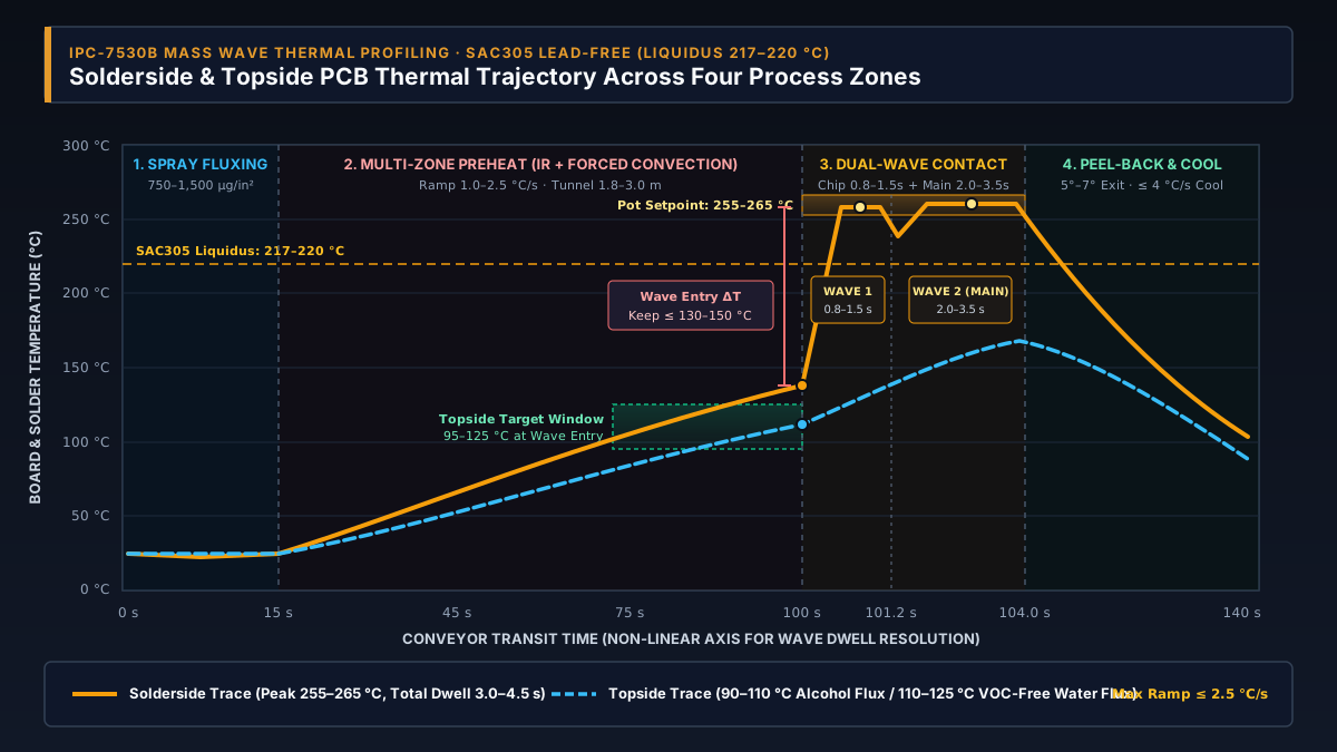
Topside temperature targets by board construction and flux vehicle
Because underside thermocouples are directly exposed to radiant heaters while internal copper planes shield the component side, process engineers control wave preheat by measuring the topside PCB temperature right before the board contacts Wave 1:
- Alcohol-based no-clean flux on standard double-sided PCBs (
1.6 mmthick): Target 90–110 °C (194–230 °F) topside. - VOC-free water-based flux on double-sided or moderate multilayer PCBs: Target 110–125 °C (
230–257 °F) topside. Because water has a higher boiling point (100 °C) and more than double the latent heat of vaporization of isopropanol, entering the wave below105–110 °Cleaves residual moisture inside PTH barrels that flashes to steam upon wave contact. - Heavy multilayer boards (
>= 8 layersor heavy internal ground planes): Target 115–135 °C topside (within flux thermal stability limits) using topside + bottomside forced convection so the internal copper planes do not chill the molten solder halfway up the barrel. - Thermal ramp rate limit: Maintain the preheat slope between 1.0 and 2.5 °C/s, with a strict maximum of 2.0–3.0 °C/s per Bourns semiconductor wave soldering recommendations and IPC-7530B guidelines. Slopes above
3.0 °C/sinduce tensile thermal stress in multilayer ceramic capacitors (MLCCs) and warp glass-epoxy laminate above its glass transition temperature (Tg). - Solderside-to-pot thermal shock (
Delta T): Keep the instantaneous temperature jump between the PCB underside exiting preheat and the molten solder pot at or below 130–150 °C. For a260 °CSAC305 pot, the solderside laminate should enter the chip wave at120–135 °C.
Infrared vs. forced-convection preheat coupling
As compared in our guide to reflow oven heating methods, different emitter technologies couple heat into a traveling board at different rates:
- Short-wave quartz IR emitters: Deliver rapid filament response (
< 2–3 s) and deeper radiative penetration into FR-4 epoxy, ideal for Zone 1 initial ramp-up or dynamic power switching between boards on Kurtz ErsaPOWERFLOWand Vitronics SoltecDelta 5lines. - Medium-wave IR and Calrod radiant platens: Emit longer-wavelength infrared absorbed strongly by solder mask and laminate surfaces, providing steady baseline heating across Zones 1 and 2.
- Forced air convection modules: Blow heated air or nitrogen into PTH barrels and across high-thermal-mass components, eliminating line-of-sight infrared shadowing behind tall connectors or selective wave pallets.
Worked example: Sizing active preheat tunnel length for a 1.4 m/min line
Suppose a manufacturing line must run an 8-layer industrial controller PCB using a VOC-free water-based flux at a required conveyor speed v_conveyor = 1.40 m/min (23.33 mm/s) to match upstream SMT placement takt time.
- Ambient board entry temperature
T_start = 25 °C - Required topside PCB temperature at wave entry
T_preheat = 118 °C(Delta_T_preheat = 118 - 25 = 93 °C) - Target safe thermal ramp rate
R_ramp = 1.50 °C/s(allowing a20%thermal-lag margin for internal copper ground planes)
Step 1 — Calculate the required residence time t_preheat inside the active preheat tunnel:
t_preheat = (Delta_T_preheat / R_ramp) * 1.20 = (93 °C / 1.50 °C/s) * 1.20 = 62.0 s * 1.20 = 74.4 sStep 2 — Multiply residence time by conveyor velocity v_conveyor = 23.33 mm/s to determine minimum active preheat tunnel length L_preheat:
L_preheat = v_conveyor * t_preheat = 23.33 mm/s * 74.4 s = 1,736 mm (1.74 m)A compact 1,200 mm 2-zone preheater at 1.40 m/min provides only 1,200 / 23.33 = 51.4 s of residence, forcing an average ramp rate above 2.17 °C/s (and peak underside IR spikes above 3.2 °C/s) or requiring the operator to slow the conveyor to 0.97 m/min. Specifying an 1,800 mm (3-zone) or 2,400 mm (4-zone) modular preheat tunnel (such as an Ersa POWERFLOW PRO/N2 XL, Electrovert Electra, or SEHO PowerWave N2) holds the 1.50 °C/s slope comfortably at 1.40 m/min.
Rule of thumb: If your required preheat residence time exceeds 65 s at your target conveyor speed, add a fourth preheat zone (>= 2,100–2,400 mm active length) or install topside forced-convection hoods rather than driving bottomside IR radiator setpoints above 450 °C, which scorches bottom solder mask while leaving internal ground planes cold.
Takeaway: Size preheat tunnel length from L_preheat = v_conveyor * t_preheat so the board hits 95–125 °C topside without breaching the 2.5 °C/s ramp ceiling.
Stage 3: How do dual-wave nozzle geometry, contact length, and conveyor angle govern joint formation?
Once preheated, the board travels across the molten solder pot. For lead-free SAC305 (Sn96.5/Ag3.0/Cu0.5, solidus 217 °C / liquidus 220 °C per AIM Solder TDS NF7; see reading solder alloy melting endpoints), the solder pot typically operates at 255–265 °C (491–509 °F). This provides 35–45 °C of superheat above liquidus—higher than the 25 °C minimum joint superheat noted in IPC-7530B because the molten wave must heat the PTH barrel walls and component leads via conduction in just 3.0–4.5 s of contact.
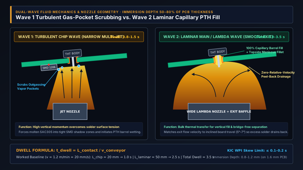
Wave 1 (turbulent chip wave) vs. Wave 2 (laminar smooth wave)
Why does modern wave soldering equipment pump two distinct waves from the same pot?
- Wave 1 — Turbulent Chip Wave (
0.8–1.5 sdwell): Pumped through a narrow nozzle with oscillatory rows or multi-jet perforations, the chip wave produces a high-velocity vertical stream. When bottom-side gull-wing ICs, SOT packages, or passive0603/1206chips are glued to the underside of the PCB, their bodies create hydrodynamic “shadow zones” where surface tension prevents a smooth wave from wetting the pads and where vaporized flux collects in gas pockets. The turbulent jet breaks through the gas boundary layer, scrubs outgassing bubbles away from SMD terminations and PTH barrel entrances, and initiates metallic wetting. Because the exit of a turbulent jet is unstable, boards exiting Wave 1 alone often carry pin-to-pin bridges and icicles. - Wave 2 — Laminar Smooth / Lambda Wave (
2.0–3.5 sdwell): Immediately after the chip wave, the board enters a wide, low-turbulence bidirectional wave (Lambda,OptiWave,DwellFlex, orVarioWave). The laminar wave acts as a continuous thermal reservoir that heats the PTH barrel and pin above220 °Cso molten SAC305 rises to the topside land by capillary pressure (Delta P = 2 * gamma * cos(theta) / r). At the trailing edge of the laminar nozzle, an exit wing or baffle shapes the solder flow backward at the same speed the inclined board moves forward.
Conveyor tilt angle, immersion depth, and zero-velocity peel-back
Bridges and icicles are eliminated at the exact point where the trailing pins leave Wave 2:
- Conveyor incline angle (
5°–7°standard within4°–7°adjustment range): Tilting the conveyor upward at5°–7°utilizes gravity to help molten solder drain back into the pot as the board separates from the laminar wave. Lowering the angle toward4°–5°lengthens the wetted contact footprintL_contact(increasing dwell time for thick backplanes), whereas steepening the angle toward6°–7°sharpens the peel-back angle to strip excess solder off fine-pitch connectors. - PCB immersion depth (
50–80%of board thickness): On a standard1.6 mm(62 mil) laminate, adjust pump RPM and closed-loop wave height sensors (such as Electrovert’sExactaWave) so the board immerses 0.8–1.2 mm into the wave crest. Immersing shallower than50%starves wetting pressure and increases sensitivity to board warpage; immersing deeper than80%risks flooding molten solder onto the topside through tooling holes or board edges. - Nitrogen inerting (
50–500 ppm O2): Enclosing the wave tunnel in nitrogen reduces liquid solder surface tension and prevents rapid tin-oxide skin formation at separation. As AIM Solder’s dross control documentation and Vitronics Soltec’s inert-atmosphere studies show, nitrogen cuts oxide dross by50–90%, improves PTH vertical fill with milder low-solids fluxes, and keeps the exit peel-back clean.
Worked example: Dwell time calculation and KIC WPI parallelism check
Wave contact dwell time t_dwell is governed by the kinematic relationship between the wetted contact length L_contact (in mm) along the conveyor travel direction and the conveyor speed v_conveyor (in mm/s):
t_dwell = L_contact / v_conveyorSuppose a production line runs a mixed-technology power supply board at a conveyor speed v_conveyor = 1.20 m/min:
Step 1 — Convert conveyor speed to millimetres per second:
v_conveyor = 1,200 mm / 60 s = 20.0 mm/sStep 2 — An automated wave profiling fixture (such as a KIC Wave Process Inspection (WPI) sensor palette or tempered glass wave-contact plate) measures a turbulent chip wave contact footprint L_chip = 22 mm and a laminar main wave contact footprint L_laminar = 54 mm:
t_chip    = 22 mm / 20.0 mm/s = 1.10 s  (Target window: 0.8–1.5 s)
t_laminar = 54 mm / 20.0 mm/s = 2.70 s  (Target window: 2.0–3.5 s)
t_total   = 1.10 s + 2.70 s   = 3.80 s  (Target window: 3.0–4.5 s)
Step 3 — Check left-to-right nozzle parallelism across the conveyor width:
Suppose the KIC WPI profiler records L_laminar_left = 54 mm (2.70 s), L_laminar_center = 53 mm (2.65 s), and L_laminar_right = 46 mm (2.30 s). The left-to-right dwell skew is 2.70 - 2.30 = 0.40 s, which exceeds the <= 0.1–0.2 s (< 0.5 mm immersion depth) parallelism specification. Left unadjusted, boards on the right rail will suffer cold barrel fill while boards on the left rail risk copper knee leaching. Leveling the solder pot jacking screws until L_laminar reads 53–55 mm (2.65–2.75 s) across all three lanes restores uniform yield.
Rule of thumb: If total wave contact dwell exceeds 5.0 s at 260–265 °C on a lead-free SAC305 pot, do not slow the conveyor further to fix incomplete hole fill; instead, increase forced-convection preheat topside temperature or switch to an adjustable-contact laminar nozzle (DwellFlex / VarioWave) while capping pot temperature at 260 °C.
Takeaway: Measure L_chip and L_laminar directly across left, center, and right conveyor lanes; pump RPM numbers on the HMI screen do not guarantee a level wave.
How do IPC-A-610 Section 7 and J-STD-001 judge through-hole joints and bath purity?
Every wave-soldered assembly is inspected against IPC-A-610 (Acceptability of Electronic Assemblies, Section 7: Through-Hole Technology—complementing the Section 8 surface-mount fillet rules verified upstream by 3D automated optical inspection in SMT assembly) and controlled in production under IPC J-STD-001 (Requirements for Soldered Electrical and Electronic Assemblies, with Revision J released in April 2024).
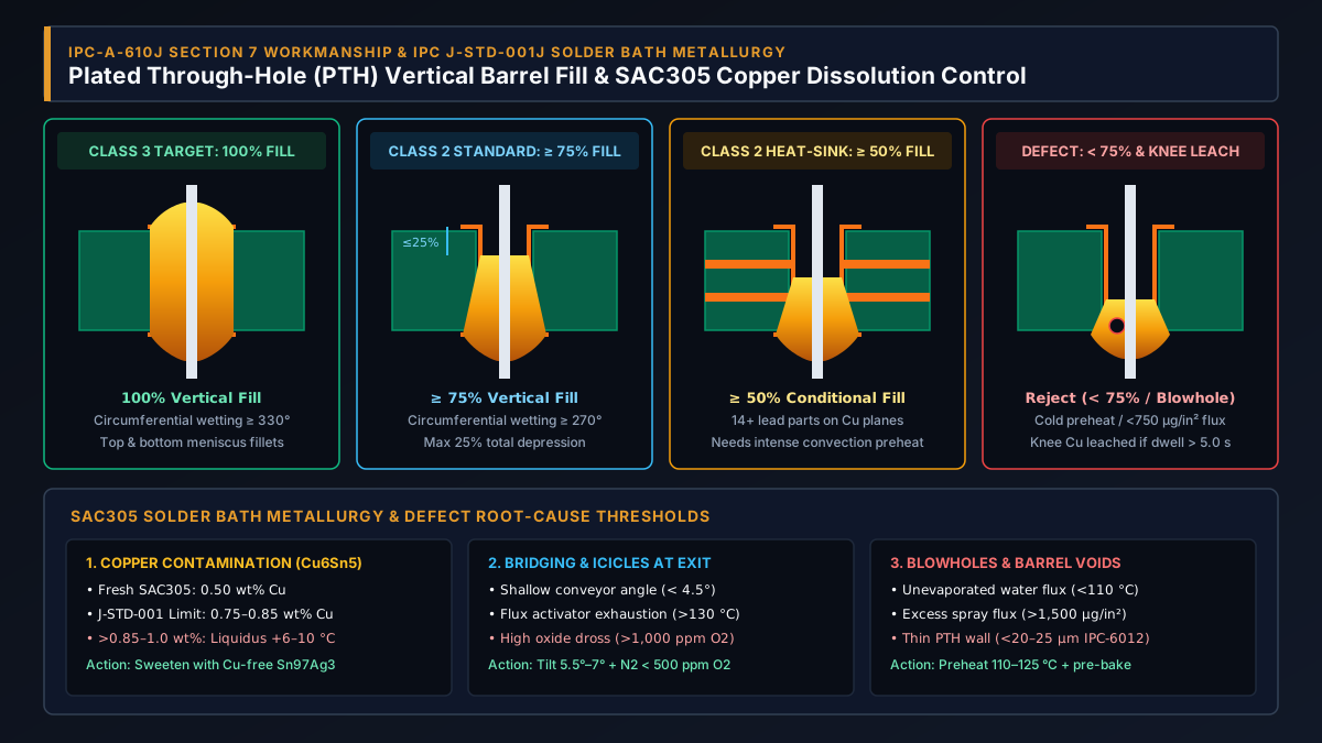
IPC-A-610 Section 7 vertical barrel fill and wetting criteria
| Inspection Parameter | IPC Class 1 (General Consumer) | IPC Class 2 (Dedicated Service / Industrial) | IPC Class 3 (High-Reliability / Aerospace / Medical) |
|---|---|---|---|
| Standard PTH Vertical Barrel Fill | Wetting of lead and barrel required; vertical fill % not a hard minimum | Minimum 75% vertical fill (max 25% combined top + bottom depression) | Minimum 75% vertical fill (100% full barrel fill + topside fillet targeted on signal barrels) |
| Thermal / Ground Plane Exception | Wetting of lead and barrel wall required | Minimum 50% vertical fill permitted on multi-lead parts (14+ leads) tied to internal thermal/ground planes with topside lead wetting | Minimum 75% vertical fill required even on internal thermal/heat-sink planes |
| Circumferential Wetting (Lead & Land) | Evident wetting of lead to barrel | Minimum 270° circumferential wetting on solder destination and source sides | Minimum 330° circumferential wetting on solder destination and source sides |
| Exposed Copper at Barrel Knee | Allowed if wetting is continuous | Allowed only within depression limit; no fractured fillet | Topside land meniscus fillet required; excessive knee thinning rejected |
When a thick multilayer board (>= 12 layers or heavy internal copper planes) cannot achieve 75% vertical fill in a mass wave pallet without overheating nearby SMT parts, review whether those specific connectors belong on an inline selective soldering machine (see when selective soldering is the better fit).
IPC J-STD-001 and AIM Solder bath copper contamination physics
A molten wave solder pot is an active metallurgical reactor. Because lead-free SAC305 contains 96.5 wt% tin (compared to 63 wt% tin in eutectic Sn63/Pb37; see alloy selection in our solder paste guide) and runs at 255–265 °C, it dissolves exposed copper from PTH barrel walls, barrel knees, and OSP/immersion-silver pads at more than twice the rate of tin-lead solder:
- Starting composition vs. upper limit: Fresh SAC305 bars contain 0.50 wt% Cu. Under IPC J-STD-001 and AIM Solder bath maintenance standards, the maximum copper contamination limit in a SAC305 wave pot is 0.75–0.85 wt% Cu (with up to
1.0 wt% Cupermitted by user-supplier agreement on high-thermal-mass boards, and1.2 wt% Cuflagged by AIM as the severe defect ceiling; by contrast,Sn63/Pb37pots cap copper at0.30 wt%). - Intermetallic needle precipitation (
Cu6Sn5): According to the ternarySn-Ag-Cuphase diagram, each0.1 wt%increase in copper above the0.50 wt%eutectic point raises the alloy liquidus temperature by roughly 2.0–2.5 °C. Once bath copper exceeds 0.85–1.0 wt%, liquidus rises by6–10 °C, reducing effective superheat at260 °Cand precipitating needle-likeCu6Sn5intermetallic crystals. The molten wave becomes viscous and sluggish, causing gritty fillets, icicles, pin-to-pin bridging, and incomplete vertical hole fill. - Pot sweetening calculation: Sample the molten solder pot every
2–4 weeks(100–160 operating hours) for XRF or atomic absorption spectroscopy. When copper reaches 0.80–0.85 wt%, drain a calculated fraction of the pot and replenish (“sweeten”) with copper-free Sn97Ag3 (0.0 wt% Cu) top-off ingots. For example, in a600 kgErsaPOWERFLOW PROpot reading0.84 wt% Cu, replacing120 kg(20%of bath mass) with copper-freeSn97Ag3dilutes bath copper to(480 * 0.84 + 120 * 0.0) / 600 = 0.67 wt% Cu, restoring fluidity right in the0.55–0.75 wt%equilibrium band.
Wave soldering defect troubleshooting matrix
| Observed Defect | Primary Process / Metallurgical Root Causes | Corrective Engineering Actions |
|---|---|---|
Insufficient Vertical Hole Fill (< 75% Class 2/3) |
1. Spray flux solids < 750 µg/in² or poor air-knife barrel penetration2. Topside preheat < 95 °C (< 115 °C on heavy Cu planes), freezing solder mid-barrel3. Laminar wave dwell < 2.0 s or shallow immersion (< 50% PCB thickness)4. SAC305 bath copper > 0.85 wt% raising viscosity |
1. Verify 750–1,500 µg/in² solids deposition and adjust air-knife angle2. Increase forced-convection preheat soak to reach 110–125 °C topside3. Lengthen laminar wave contact ( DwellFlex/VarioWave) to achieve 3.0–4.5 s total dwell4. Sweeten pot with copper-free Sn97Ag3 bars to bring Cu below 0.75 wt% |
| Pin-to-Pin Bridging & Icicles | 1. Flux activators thermally exhausted before wave exit (> 130–140 °C preheat)2. Conveyor angle too shallow ( < 4.5°) or exit flow mismatch3. Elevated bath copper ( > 0.85 wt%) or heavy oxide dross entrainment (> 1,000 ppm O2)4. Fine-pitch connector rows oriented perpendicular to wave travel without thief pads |
1. Trim preheat peak or switch to higher-thermal-stability lead-free wave flux 2. Increase conveyor tilt to 5.5°–7.0° and tune laminar exit baffle velocity3. Skim dross compartment, verify N2 tunnel ( 50–500 ppm O2), and dilute pot Cu4. Add trailing solder thief pads or rotate fine-pitch rows parallel to travel |
| Blowholes & Pinholes (Outgassing Voids) | 1. Unevaporated water carrier in VOC-free flux flashing to steam at 260 °C2. Excessive spray flux deposition ( > 1,500 µg/in²)3. Absorbed laminate moisture outgassing through thin ( < 20–25 µm) or voided PTH copper plating |
1. Raise topside preheat to 110–125 °C while holding slope <= 2.0 °C/s2. Reduce spray fluxer flow rate and verify nozzle atomization 3. Pre-bake hygroscopic bare PCBs ( 105–125 °C for 2–4 h) and audit fabricator PTH copper wall thickness (>= 20–25 µm per IPC-6012 Class 2/3) |
| PTH Barrel Knee Copper Dissolution | 1. Excessive total wave contact dwell (> 5.0 s) or pot temperature > 265–270 °C2. High copper leaching rate of fresh, low-copper high-tin solder during turbulent + laminar exposure |
1. Cap SAC305 pot at 255–265 °C and keep total dwell within 3.0–4.5 s2. Maintain bath Cu in the 0.55–0.75 wt% equilibrium band or use micro-alloyed Ni-stabilized wave alloys where specified |
| Solder Balls & Underside Spatter | 1. Excessive flux solvent/water spattering on contact with Wave 1 2. Solderside-to-pot Delta T > 150 °C or turbulent chip wave jet set too high3. Ultra-low oxygen ( < 50 ppm O2) on certain matte solder masks reducing solder pullback |
1. Increase preheat solvent evaporation and verify pre-bath heater operation 2. Dampen Wave 1 pump RPM and verify 0.8–1.5 s chip dwell3. Tune N2 atmosphere to 150–400 ppm O2 balance point |
Rule of thumb: If bridging and icicles suddenly spike across multiple board part numbers on the same shift without a recipe change, test solder bath copper concentration and check the laminar exit baffle for dross buildup before altering conveyor speed or flux flow.
Takeaway: Control vertical hole fill and bridging by treating flux solids (750–1,500 µg/in²), topside preheat (95–125 °C), dual-wave dwell (3.0–4.5 s), and SAC305 copper purity (< 0.85 wt%) as one coupled system.
Related reading
- Wave soldering vs reflow: choose a process for each part — Our pillar decision framework comparing reflow, mass wave, selective dip/nozzle, and hand soldering.
- Reflow oven types and how to choose one for PCB assembly — Forced convection, infrared, and vapor-phase oven architectures plus heated-tunnel length sizing.
- Reflow soldering process stages and temperature profile — Preheat, soak, reflow, and cooling thermal limits for surface-mount paste assemblies.
- ROL0 no-clean vs water-soluble solder flux — How IPC J-STD-004 flux activity codes govern residue safety and post-solder cleaning.
- Automated optical inspection (AOI) in SMT assembly — Pre-reflow vs. post-reflow 3D Moiré AOI placement, IPC-A-610 Section 8 SMD criteria, and IPC-CFX closed-loop feedback.
- Electronics manufacturing guides — Browse all PCB assembly, soldering, and inspection explainers on the EMT WorldWide blog.