Leaving every module pull-up in place can hold SDA above the low level the weakest chip can drive, and the next ACK fails. Calculate one effective resistance for the resistors that share a node, compare it with the sink-current floor and the capacitance ceiling, and remove or add a resistor only after that comparison.
The short answer: On one direct I2C connection, pull-ups to the same supply add in parallel. Record each module’s resistor, its supply, whether the module is powered and enabled, and which segment it sits on. Combine only the resistors on the node you are checking. Texas Instruments SLVA689A, revised October 2026, sets the minimum resistance from supply, maximum low level, and sink current, and the maximum resistance from rise time and bus capacitance. Keep the set when the parallel value sits between those limits, then confirm the released high, the rise from 0.3 to 0.7 of the pull-up supply, and the driven low. A direct parallel connection puts every selected resistor on one electrical node. A switch or a buffer gives each side its own node.
| Input | Value used in the formulas | Why it matters |
|---|---|---|
| Pull-up supply, VCC or VDD | From the rail the resistor ties to | Sets both the high level and the minimum resistance |
| VOL(max) and IOL | From the weakest device’s datasheet, or from the mode table you name | A strong pull-up (small resistor) can stop that device from producing a valid low |
| Rise time, tr | 1000 ns standard, 300 ns fast, 120 ns Fast-mode Plus in TI Table 2-1 | A weak pull-up can miss this edge |
| Bus capacitance, Cb | Wire, connections, and pins on this segment | NXP UM10204 section 7.1 defines Cb this way; the other side of a buffer is a different Cb |
| Which resistors are in Req | Audit columns below | An unpowered module or an unselected channel stays out of this sum |
The cover photo is an illustration of modules and discrete resistors on a wired bus. It is not a scope capture, a named board, or a test result.
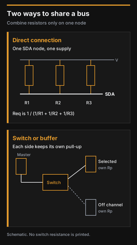
Figure 1. A direct connection shares one node. A switch keeps a pull-up on the master side, the selected channel, and any channel that still has a device. Schematic. No switch resistance is printed.
Other hardware notes on this site are listed on the article index.
Which pull-ups are actually on this node?
The audit row is the job. A silkscreen value, a powered regulator, and a switch channel are three different facts. Write them before you add the resistances.
Scroll the table sideways on a phone. Copy one row per module. Leave every cell blank until you have the schematic or a measurement of that part. A blank internal-pull-up cell is an unknown. It is not zero, and it is not a default resistor.
| Module | SDA pull-up | SCL pull-up | Pull-up supply | Powered | Enable or channel | Segment | Count in this Req |
|---|---|---|---|---|---|---|---|
- SDA pull-up and SCL pull-up. Measure each populated resistor with one end lifted, or read the value from the module schematic and confirm the part. Do SDA and SCL as separate sums when the resistors differ. An internal pull-up belongs in the cell only after you copy its resistance from that MCU’s datasheet. This page does not publish one internal value for every MCU.
- Pull-up supply. Write the rail the resistor goes to. TI’s introduction notes that open-drain I2C lets devices on different supply rails share a bus. Resistors that do not share a supply do not share one high level.
- Powered, and enable or channel. A pull-up behind an unpowered regulator is off the bus. On a switch, write the channel and whether it is selected.
- Segment. Use a plain label: direct node, master side, channel 0, or the far side of a buffer. Only a “yes” in the last column enters Req for the calculation you are doing now.
- Count in this Req. Yes, no, or unknown. Unknown stops the arithmetic. Do not guess a module that you have not opened.
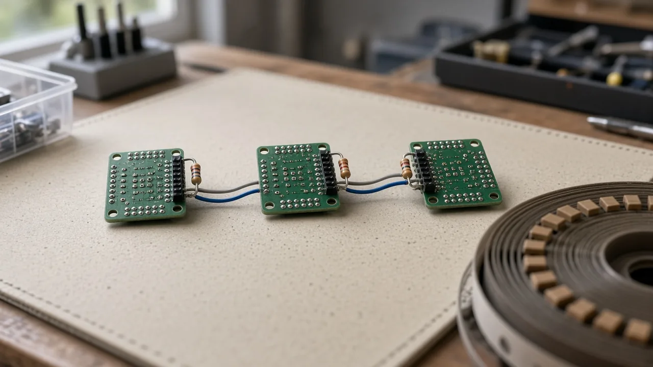
Illustration of discrete resistors next to a header on a wired bus. Not a scope capture, a named board, or a measured result.
Takeaway: Req uses only the resistors whose audit row says they are powered, enabled, and on this segment.
How do you combine pull-ups on one direct connection?
A direct parallel connection puts every selected resistor on one electrical node. For that node:
Req = 1 / (1/R1 + 1/R2 + … + 1/Rn)
When the resistors are equal, Req = R / n. Run the sum once for SDA and once for SCL.
Texas Instruments E2E, in the PCA9548A thread, is the place to stop treating every switch as that sum. Johnny Guo asked whether a selected channel is simply 4.7 kΩ in parallel with 4.7 kΩ. Miguel Robertson’s first reply says the resistances are in parallel when the switch is on, and that the device is a FET switch with low on-state resistance. His later replies narrow that statement. The switch conducts when one side is pulled low, so a high is not passed through the same low-resistance path. Each side is pulled up by its own resistors to its own supply, which is how the two sides can sit at different high levels. Both sides need a pull-up. A high that exists only on SDA/SCL does not create the high on SD0/SC0.
Parker Dodson, answering a TS3A24159 question, states the same boundary in circuit terms: a pull-up serves one node, and the switch’s resistance and capacitance split the bus into nodes. Each node needs its own pull-up. The thread does not give an on-resistance to drop into Req. Read Ron from the switch datasheet if your low-level budget needs it. This page does not invent that number.
NXP UM10204 section 7.2.3, Rev. 7.0, 1 October 2021, draws the buffer case. A buffer, multiplexer, or switch divides the bus into smaller segments. In the PCA9515 example, each segment is allowed the maximum capacitance, so the whole bus can carry twice that maximum. Figure 43 shows 400 pF on each side of the buffer. Add those two figures only if you are describing two segments. Do not add them into one Cb for one Rp. NXP also says a buffer adds delay, a buffer delay plus another transition on each edge, and that this lowers the maximum frequency and introduces its own VIL and VOL limits. Those limits come from the buffer datasheet. This page does not build an equivalent model for an unknown buffer or level shifter.
NXP section 7.2.4 is a different circuit again: a switched pull-up on the same segment, turned on during the edge. It is not a channel switch that separates nodes. Leave that circuit on the NXP page unless you are building that exact arrangement.
Takeaway: Use the parallel formula for resistors that share one direct node. Give every side of a switch or buffer its own pull-up and its own capacitance.
What sets the minimum and maximum resistance?
TI SLVA689A section 2, checked on the rendered October 2026 PDF, prints:
Rp(min) = (VCC − VOL(max)) / IOL
A smaller resistor is a stronger pull-up. TI says a strong pull-up can stop the pin from driving a valid low. The VOL that the receivers still read as low is what sets Rp(min).
The ceiling comes from capacitance and rise time. TI equation (5) prints:
tr = 0.8473 × Rp × Cb
TI equation (6) prints:
Rp(max) = tr / (0.8473 × Cb)
NXP section 7.1 derives the 0.8473 factor from the thresholds it names. With V(t) = VDD (1 − e^(−t/RC)), the time to 0.3 VDD is 0.3566749 × RC and the time to 0.7 VDD is 1.2039729 × RC. The difference is 0.8473 × RC. NXP then writes the same ceiling, Rp(max) = tr / (0.8473 × Cb), with tr from its Table 10 and Cb estimated for the bus. NXP defines bus capacitance as the total capacitance of wire, connections, and pins.
The October 2026 PDF’s equation (3) does not print a readable Cb in the exponent; the text layer is garbled there. Equation (4) uses Cb, and equation (5) states the 0.8473 product. The formulas above are the ones used on this page.
TI Table 2-1, same revision, lists the mode limits the example uses:
| Parameter | Standard-mode max | Fast-mode max | Fast-mode Plus max |
|---|---|---|---|
| Rise time of SDA and SCL | 1000 ns | 300 ns | 120 ns |
| Capacitive load, Cb | 400 pF | 400 pF | 550 pF |
| VOL at 3 mA, VCC > 2 V | 0.4 V | 0.4 V | 0.4 V |
| VOL at 2 mA, VCC ≤ 2 V | — | 0.2 × VCC | 0.2 × VCC |
NXP section 7.1 states a different sink current for Fast-mode Plus: 3 mA for Standard-mode and Fast-mode, or 20 mA for Fast-mode Plus. Do not swap those currents into TI’s table, and do not swap TI’s 3 mA row into a Fast-mode Plus design that you are checking against NXP. The weakest device on your audit wins. If its datasheet allows less than the mode-table current, use the datasheet current. Rp(min) gets larger as IOL gets smaller, so the floor moves up and fewer strong pull-ups still fit.
TI section 3 is the choice inside a window that still has room: a smaller resistor gives a faster edge because the RC delay is smaller, and a larger resistor draws less current while the line is low.
Takeaway: Rp(min) comes from the weakest sink. Rp(max) comes from tr and the capacitance of this segment only.
What does the worked example assume?
The numbers in this section are a calculation example. They are not a measurement of a board. The 4700 Ω parts are assumed module values so the arithmetic has an input. Replace them with the resistors on your audit.
Shared assumptions, taken from TI SLVA689A section 4 and Table 2-1:
- Fast-mode, VCC = 3.3 V, Cb = 200 pF, tr maximum = 300 ns.
- VOL(max) = 0.4 V at IOL = 3 mA, the table row for VCC above 2 V.
- TI’s printed results for those inputs: Rp(max) = 1.77 kΩ and Rp(min) = 966.667 Ω.
- Every resistor in a row sits on one direct SDA node, powered and enabled, tied to that same 3.3 V rail. Repeat the sum for SCL when its resistors differ.
Checking the printed arithmetic against equation (6) and equation (1): 300 ns / (0.8473 × 200 pF) = 1770 Ω, which TI rounds to 1.77 kΩ. (3.3 V − 0.4 V) / 3 mA = 966.667 Ω. TI says any available resistor between those two values can be selected, with the choice based on power and speed. That sentence is about one resistor on that example bus. It is not a claim that one value works on every bus.
Scroll the comparison sideways on a phone. The last column is the decision.
| Assumed resistors on one direct node | Req | Against 966.667 Ω to 1.77 kΩ | What to do next, under these assumptions |
|---|---|---|---|
| One 4700 Ω | 4700 Ω | Above 1.77 kΩ | Too weak for 200 pF at 300 ns. Add a resistor on this same node, or lower Cb, then recalculate. 4700 Ω in parallel with an assumed 2200 Ω is 1498.6 Ω, inside the window. |
| Three 4700 Ω | 1566.7 Ω | Inside | Keep all three, then run the waveform checks. |
| Four 4700 Ω | 1175 Ω | Inside | Keep all four, then run the waveform checks. |
| Five 4700 Ω | 940 Ω | Below 966.667 Ω | Too strong for the 3 mA, 0.4 V floor. Remove one. Four 4700 Ω resistors return 1175 Ω. |
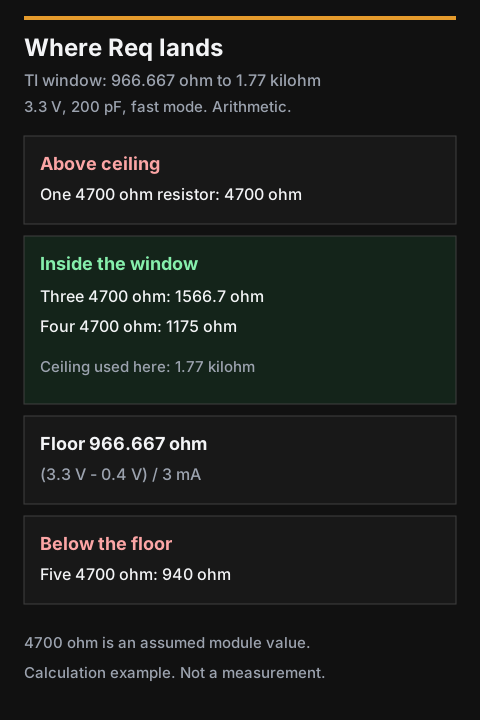
Figure 2. The same assumed 4700 Ω parts land above, inside, or below TI’s printed window. Calculation example. Not a measurement.
Equal resistors divide. 4700 / 3 = 1566.7 Ω. 4700 / 4 = 1175 Ω. 4700 / 5 = 940 Ω. The parallel of 4700 Ω and 2200 Ω is 4700 × 2200 / (4700 + 2200) = 1498.6 Ω.
Apply equation (6) to the fast-mode maxima in Table 2-1, 300 ns and 400 pF, and the ceiling falls to 885 Ω. That sits below the 966.667 Ω floor from the same table at 3.3 V and 3 mA. Under those two limits together, no single resistor satisfies both. A bus near 400 pF on fast-mode needs a lower capacitance, a mode whose rise time is longer, a sink current the datasheet actually allows, or a split into segments. NXP section 7.2 lists lower clock rate, stronger drivers, buffers, and a switched pull-up as the ways to live with extra capacitance. Pick one from the device you are using. Do not paper over a closed window with a favorite resistor.
If those three 4700 Ω resistors sit on three PCA9548A channels, 1566.7 Ω is the wrong high-level model for the selected channel. Miguel Robertson’s later replies put the parallel combination on the low path, when the switch is on and a device is driving low. The high on each side is that side’s own pull-up. An unselected channel is another node. Parker Dodson’s point, and Clemens Ladisch’s note that a disconnected segment floats, both say the off channel still needs a pull-up if devices remain on it. Clemens adds that the resistors on inactive segments do not have to be the low value used for speed.
Takeaway: Under the stated fast-mode assumptions, three or four of the assumed 4700 Ω resistors stay inside TI’s window, one is too weak, and five are too strong. A switch moves the third resistor onto a different node.
Which measurement decides keep or remove?
The table above does not decide the board. It decides which resistors you take to the bench. Accept the set only when the arithmetic window and the waveform checks both pass. A value inside the window on paper still fails when Cb was larger than the estimate.
- Fill the audit. Lift one end of a populated resistor, or read it from the schematic and measure the part, so you record that resistor rather than the parallel combination.
- Mark a resistor “no” for this Req when its module is unpowered, its enable is off, or its switch channel is unselected. Mark “unknown” when you cannot tell, and stop.
- Compute Req from the “yes” rows, separately for SDA and SCL.
- Compute Rp(min) = (VCC − VOL(max)) / IOL from the weakest device’s datasheet at this supply. If you use a mode table instead, write the document, the revision, and the row. TI’s 3 mA and NXP’s 20 mA Fast-mode Plus row are different inputs.
- Estimate Cb for this segment only: wire, connectors, and pins, which is NXP’s definition. Do not add the capacitance on the far side of a buffer.
- Compute Rp(max) = tr / (0.8473 × Cb) with the rise-time maximum for the mode you are using.
- When Req is below Rp(min), remove or disconnect a module pull-up and recalculate. Leave a pull-up on every node that still has a device.
- When Req is above Rp(max), the combination is too weak for that capacitance. Add a resistor on this same node, or shorten the wiring, and recalculate. Removing a resistor makes Req larger and the rise slower.
- Then measure. The steps above are still arithmetic until this point.
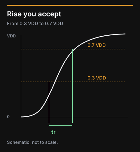
Figure 3. Accept the edge when the time from 0.3 VDD to 0.7 VDD is within the rise-time maximum you used. Schematic. Not a scope capture.
| Check | What you look at | Accept when |
|---|---|---|
| Idle high | Released SDA and SCL on this node | The line sits at this node’s pull-up supply |
| Rise | Time from 0.3 times that supply to 0.7 times that supply | The time is at or under the tr maximum used in Rp(max) |
| Low | The weakest device you used for Rp(min), driving the line low | The low is at or under the VOL(max) in the formula |
| Other side of a switch | Released line on the selected channel | That side reaches its own pull-up supply |
| Unselected channel | Devices that stay attached while the channel is off | Those devices still have a pull-up on their own node |
Miguel Robertson’s later replies are the reason the switch row exists. If SDA/SCL is pulled up and SD0/SC0 is not, the channel side does not inherit the master-side high. Parker Dodson reports the same class of trouble when pull-ups are missing on one side of TS3A24159: the switch splits the bus, and each node needs its own resistor.
Common mistake: Treating the first PCA9548A reply as the whole answer. The parallel sum applies when the switch is on and the bus is driven low. The high on each side is still that side’s own pull-up. Use both parts of that thread before you delete a channel resistor.
Takeaway: Remove a pull-up when the driven low is too high. Add one, on the same node, when the 0.3-to-0.7 rise is too slow.
When this calculation does not apply
- One internal pull-up for every MCU. The audit cell takes the resistance from that part’s datasheet. A range in the datasheet means you record both ends: the lower resistance is the one that can break Rp(min), and the higher resistance is the one that can break Rp(max).
- An unknown buffer or level shifter. Stop at the segment boundary in NXP section 7.2.3. The delay, VIL, and VOL of that part come from its datasheet.
- A favorite fixed resistor. TI’s 966.667 Ω to 1.77 kΩ window belongs to 200 pF, 3.3 V, and the fast-mode row in section 4. At the fast-mode table maxima, 300 ns and 400 pF, equation (6) evaluates to 885 Ω, which is already under the 966.667 Ω floor. The window can close.
- Fast-mode Plus copied from the wrong row. NXP’s 20 mA and TI’s 3 mA row are both in the sources. They are not interchangeable. Write the one your design is using.
- A switched pull-up that only strengthens the edge. NXP section 7.2.4 is that circuit, on one segment. It is a different problem from several modules in parallel, and from a channel switch.
- Two supplies shorted together on one direct node. TI allows different rails when the open-drain connection and the pull-ups are arranged for that. Resistors to two supplies on one shorted node are outside the single-supply sum on this page.
Takeaway: Keep the audit, recompute both limits from the datasheet in your hand, and split the bus when the window has no resistor left.
Method and sources
Compiled on 12 October 2026 from four public documents listed at the end of this article. No bus was wired and no edge was captured for this page. The worked resistances are arithmetic on TI’s section 4 inputs plus assumed 4700 Ω and 2200 Ω module values. Replace those assumptions with your audit before you remove a part.
SLVA689A on the TI site is revision A, February 2015 revised October 2026. Equations (1), (5), and (6), Table 2-1, and the section 4 results were checked against the rendered PDF pages, because the extracted text layer breaks the fractions. Equation (3) in that PDF does not show a clean Cb in the exponent; equation (5) is the rise-time formula used here. UM10204 is Rev. 7.0, 1 October 2021. Sections 7.1 and 7.2.3 were read from the rendered pages, including the 0.3566749 and 1.2039729 time constants and the PCA9515 segment example.
The PCA9548A thread is older than those revisions. Miguel Robertson’s first reply and his later replies are both used. The first reply alone says the resistors are in parallel when the switch is on. The later replies say the switch conducts on a low and that each side needs its own pull-up for a high. The TS3A24159 thread supplies Parker Dodson’s node rule and Clemens Ladisch’s note on a disconnected segment. Clemens is a forum participant on that thread; Parker then agrees with him. Neither reply is a substitute for the switch datasheet.
Related reading
- Article index: the list this bus calculation sits on.
- JTAG and SWD header checklist: a separate pin check when the same custom board needs a debug connector. The I2C resistors on this page are not the debug-header pulls.